
Pattern generator for nano lithography


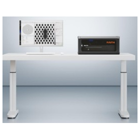
Expand the lithography function of your SEM.
The origin of RAITH's establishment, "ELPHY," is the world's most accomplished pattern generator. It supports a wide range of applications, from simple single-field drawings to complex and automated multi-layer and multi-field patterning and measurement. It is an accessory that adds nano-lithography capabilities while maintaining the original functions of existing SEM/FIB-SEM systems. By adopting RAITH's software platform "RAITH Nanosuite," it seamlessly integrates everything from CAD layout creation to automatic exposure and measurement. • System control, pattern and job preparation, automation • Seamless integration from CAD layout to automatic exposure and automatic measurement • Equipped with a professional-grade GDSII-compatible integrated design editor/viewer • Support for true 3D nano fabrication • Option to add Proximity Effect Correction (PEC) functionality • Advanced drawing strategy definition and setting capabilities • High-precision overlay/multi-layer lithography support
basic information
■High-speed and high-precision pattern placement achieved through hardware utilizing the latest FPGA technology •Sub-nanometer level pattern placement accuracy with 18/20 bit resolution •Advanced light field alignment with up to 8 reference points •Flexible scanning modes with PerfectShapes technology (reducing line edge roughness) ■Equipped with dedicated software modules to support a wide range of research and development applications •Proximity effect correction and 3D resist development simulation •3D lithography using grayscale patterns •Nano contact formation workflow •FEBIP/FIBIP functionality •Basic measurement functions ■Product lineup Maximum drawing frequency: ELPHY Plus 50MHz, ELPHY Quantum 20MHz DAC resolution: ELPHY Plus 20bit, ELPHY Quantum 18bit
Price range
Delivery Time
Model number/Brand name
ELPHY
Applications/Examples of results
Main Applications • Photonic crystals and optical resonators • Quantum effect devices, quantum wires • Grayscale lithography • FIB milling and EBL/FIB hybrid processing • Nano contact formation • Insulating film deposition by FEBID • Nanopores, silicon nanowires • CMOS circuit and device prototyping
Detailed information
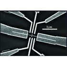
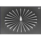
Line up(2)
| Model number | overview |
|---|---|
| ELPHY Quantum | Entry model |
| ELPHY Plus | Standard model |
catalog(1)
Download All Catalogs
Recommended products



Distributors

Hakuto Co., Ltd. is a trading company specializing in electronics and providing technical services as a technology trading company and a manufacturer of chemical industrial products, creating a rich future where people and technology coexist by identifying individual needs. Our company was established in November 1953 as a trading company engaged in the import and sale of quartz crystals. The name "Hakuto" is derived from the first character of "Brazil," the origin of quartz, and "Tokyo," representing the east. This name embodies our strong desire to grow as an international trading company that connects not only Brazil and Tokyo but also the wider world. 【Manufacturers/Products Listed on Ipros】 Asahi Kasei / Sensors, Hall elements, ICs Crystal IS / UVC (Deep Ultraviolet) LEDs IMPINJ / RAIN RFID devices, systems, software