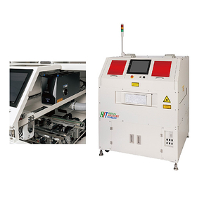
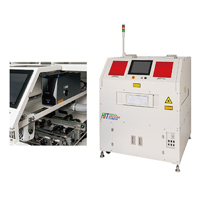
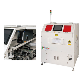
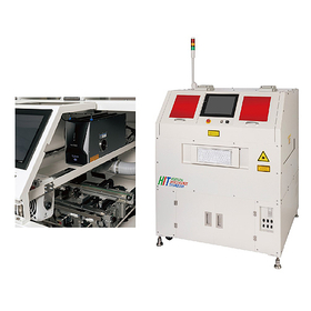
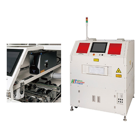
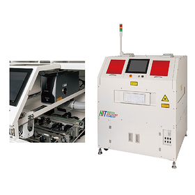
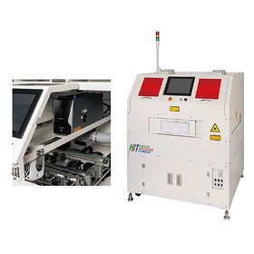
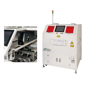
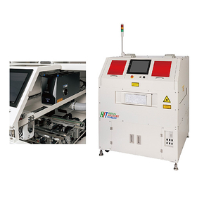
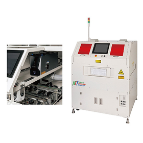
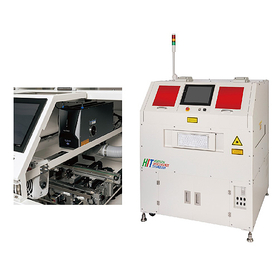
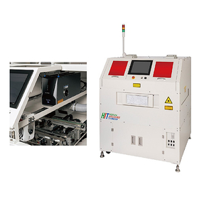
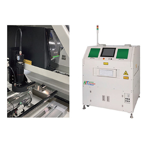
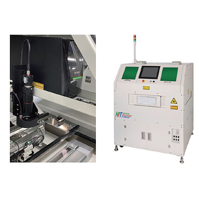
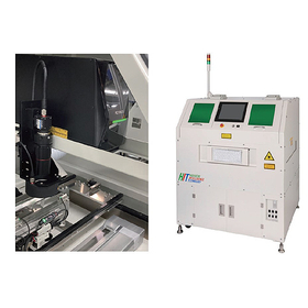
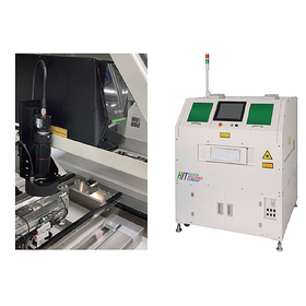
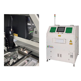
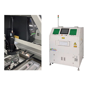
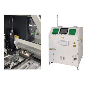
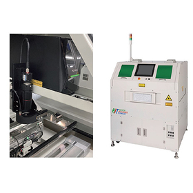
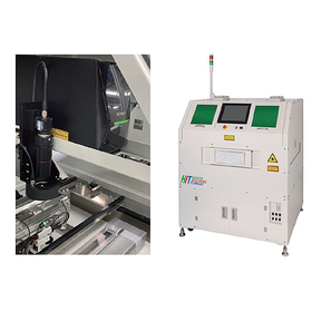
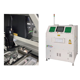
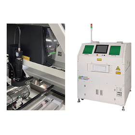
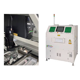
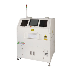
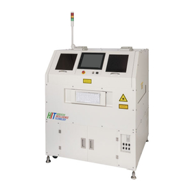
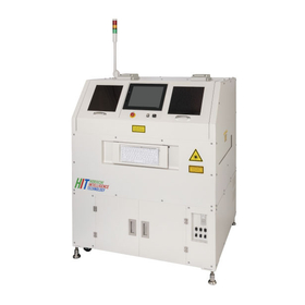
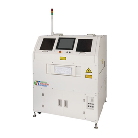
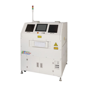
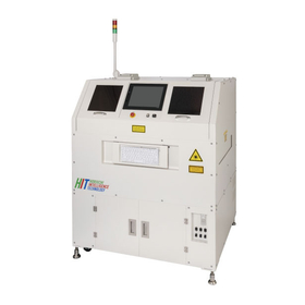
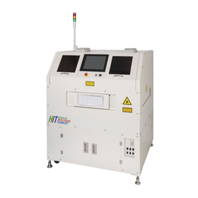
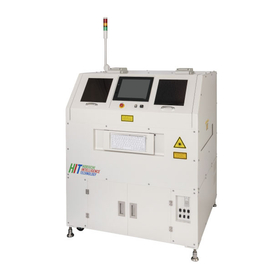
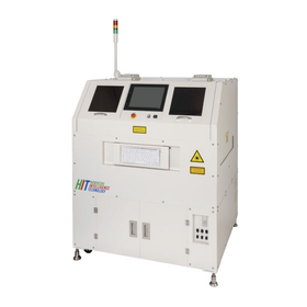
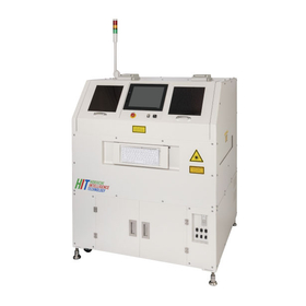
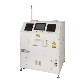
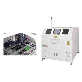
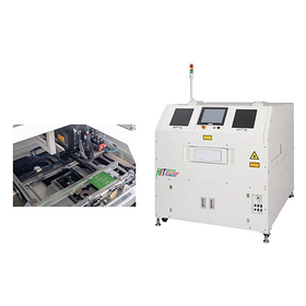
Laser marker for package use on glass epoxy/glass/ceramic substrates.
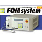
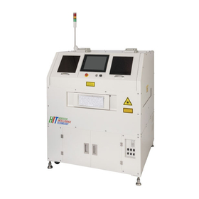
Direct marking of a unique ID that can be tracked at each stage on semiconductor package glass epoxy substrates/glass substrates/ceramic substrates.
In semiconductor package quality assurance, the ability to trace the history of each substrate unit is crucial. The LMS-K500ML is an inline laser marker that directly marks unique IDs (2D codes and characters) on FR-4 glass-epoxy, glass, and ceramic substrates for semiconductor packages, supporting substrate-level traceability in the packaging process. 【Usage Scenarios】 - Identification and lot management of individual glass-epoxy, glass, and ceramic substrates - History tracking of substrate units in the packaging (assembly) process - Precise control of printing positions avoiding fine mounting areas 【Benefits of Implementation】 - Even if defects occur in later processes, the specific substrate and lot can be identified on a unit basis - Accurate printing in narrow spaces avoiding components through XY position correction via image processing - Ensures permanent records without smudging or peeling through direct printing without labels or ink
basic information
This is a device specification based on the operation of identifying semiconductor package substrates made of glass epoxy, glass, and ceramic on a per-piece basis. 【Features】 - Equipped with a Keyence 3-axis laser marker. CO2, UV, and YVO4 light sources can be selected according to the substrate material. - Compatible materials include resin-based substrates (FR-4, CEM-3, paper phenol, etc.), as well as glass and ceramic substrates. - Alignment (XY position correction) and front/back distinction are performed using an image processing camera, avoiding the fine mounting area for printing. - Up to 999 image types can be registered. Settings are automatically recalled in conjunction with the device program number. - Supports printing of DataMatrix (ECC200), QR codes, and MicroQR codes. - Target substrates can be a maximum of 380×280mm, a minimum of 50×50mm, with a thickness of 0.6 to 2.2mm, and a weight of up to 800g. - The height of mounted components can be accommodated up to 25mm on both the top and bottom surfaces of the substrate. 【Our Strengths】 Approximately 30 years of experience in laser printing and traceability. Made in Japan, minimizing the risk of technical information leakage. We offer free test printing (work tests) on actual substrates.
Price information
For more details, please contact us.
Delivery Time
Model number/Brand name
LMS-K500ML Series (Inline laser marker capable of CO2, UV, and YVO4 for individual identification of semiconductor package substrates)
Applications/Examples of results
For more details, please refer to the PDF document or feel free to contact us.