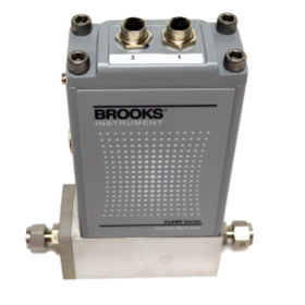
Metal Seal Mass Flow Controller/ Meter "GF100 Series"

Applications for gas flow control with excellent response speed and repeatability.
The "GF100 Series" is a metal-sealed mass flow controller/meter that achieves high purity and ultra-high purity process gas supply with excellent response speed and repeatability. It ensures high repeatability and stable performance, providing reliability that exceeds industry standards. It achieves the highest level of gas cleanliness in the industry while enhancing process flexibility and efficiency, maximizing yield and productivity. 【Features】 ■ Long-term zero point stability: less than 0.5% full scale/year ■ Settling time: less than 700 ms - 1 second ■ Maximum full-scale flow rate: 300 slpm ■ Metal-sealed flow path: surface finish options of 4µ or 10µ inch Ra ■ Corrosion-resistant Hastelloy(R) T-Rise sensor improves measurement reproducibility even with rising temperatures, among other features. *For more details, please download the PDF or feel free to contact us.
basic information
**Merits** - High-performance components that execute continuous testing in accordance with semiconductor industry standards - Reduced dry-down time during purging - Ability to set new process gases and/or ranges in under 60 seconds - Support for unexpected replacement or upgrades of metal seal MFCs, including brands - Convenient user display and independent diagnostic/service port, etc. *For more details, please download the PDF or feel free to contact us.*
Price range
Delivery Time
Applications/Examples of results
【Applications】 ■ Semiconductor etching tools ■ Thin film chemical vapor deposition (CVD) systems (CVD, MOCVD, PECVD, ALD) ■ Physical vapor deposition (PVD) systems ■ Epitaxial process systems *For more details, please download the PDF or feel free to contact us.
catalog(4)
Download All Catalogs


News about this product(8)
-

Basic Knowledge of Thin Film Technology: "Glass Coating"
A world where miniaturization and high performance are advancing daily. Mobile phones now have features that were unimaginable just a few years ago. The realization of such high performance is thanks to thin film technology, which is utilized in a wide range of applications as follows: 【Applications of Thin Film Technology】 - Microelectronics - Anti-reflective coatings for glass - Antibacterial metal coatings for medical devices - Flexible solar cells Thin film technology is defined as "the process of creating, coating, and processing thin film materials on a substrate surface." We are currently publishing basic knowledge materials on glass coatings for the glass industry! ⚫ Glass Coatings ⚫ What is Low-E Glass? ⚫ Laminating and Materials of Low-E Coatings ⚫ Application Requirements ⚫ What is Low-E Coating Technology? ⚫ Glass Coating Market Please take a moment to read it. https://mono.ipros.com/news/detail/129167/
-

Fundamental Knowledge of Thin Film Technology: "PVD and CVD Technologies"
In today's society, where miniaturization and high performance are accelerating, many products, including mobile phones, are equipped with advanced features that were unimaginable just a few years ago. Supporting this evolution is thin film technology, which is utilized in various fields. **Main Application Areas of Thin Film Technology** - Microelectronics - Anti-reflective coatings for glass - Antibacterial metal coatings for medical devices - Flexible solar cells Thin film technology refers to the process of "forming a thin layer of material on the surface of a substrate (target object) and applying coatings or processing." The materials presented in this document systematically explain the main technologies for thin film formation, namely PVD and CVD. **Contents Included** - What is PVD? - What is CVD? - What is thermal filament CVD? - What is plasma CVD? - CVD process - Range of CVD applications - Battery market - Thin film technology utilized in the battery market This document covers everything from the basics of the currently noteworthy thin film technology to advanced application examples in the battery industry. We encourage you to read it. https://mono.ipros.com/news/detail/129945/
-
Basic Knowledge of Thin Film Technology: "Glass Coating"
In today's society, where miniaturization and high performance are rapidly advancing, everyday products such as mobile phones are equipped with advanced features that were unimaginable just a few years ago. Supporting this evolution is thin film technology, which is utilized across a wide range of fields. **Main Application Areas of Thin Film Technology** - Microelectronics - Anti-reflective coatings for glass - Antibacterial metal coatings for medical devices - Flexible solar cells Thin film technology refers to the process of forming, coating, and processing extremely thin layers of material on a substrate surface. The currently available materials systematically explain the fundamental knowledge of thin film technology, particularly in the glass industry. **Content of the Materials** - Glass Coating - What is Low-E Glass? - Layering and Materials of Low-E Coatings - Application Requirements - What is Low-E Coating Technology? - Glass Coating Market This content is ideal for those looking to deepen their understanding of glass processing and coating technology. We encourage you to read it. https://mono.ipros.com/news/detail/129167/
-

【Product Information】Metal Seal Mass Flow Controller/ Meter 'GF100 Series'
Model GF100 / GF101 / GF120 / GF120XSL / GF120XSD / GF121 / GF125 / GF126 "Achieving high purity and ultra-high purity process gas supply with excellent response speed and repeatability" The GF100 series, designed for semiconductor, MOCVD, and other gas flow control applications, ensures high repeatability and stable performance, providing reliability that exceeds industry standards. With standard MultiFlo(TM) technology, it supports thousands of combinations of gas types and ranges without disconnecting from the gas line or sacrificing accuracy. It achieves industry-leading gas cleanliness while enhancing process flexibility and efficiency, maximizing yield and productivity. Applications ■ Semiconductor etching tools ■ Thin film chemical vapor deposition (CVD) systems (CVD, MOCVD, PECVD, ALD) ■ Physical vapor deposition (PVD) systems ■ Epitaxial process systems
-

Basic Knowledge of Thin Film Technology: "PVD and CVD Technologies"
A world where miniaturization and high performance are progressing daily. Mobile phones now have features that were unimaginable just a few years ago. This high performance has been made possible thanks to thin film technology, which is utilized in a wide range of applications as listed below. 【Applications of Thin Film Technology】 - Microelectronics - Anti-reflective coatings for glass - Antibacterial metal coatings for medical devices - Flexible solar cells Thin film technology is defined as "the process of creating, coating, and processing thin film materials on a substrate surface." 【PVD and CVD Technologies】 - What is PVD? - What is CVD? - What is Thermal Filament CVD? - What is Plasma CVD? - CVD Process - Range of CVD Applications - Battery Market - Thin Film Technology Used in the Battery Market Please take a moment to read it. https://mono.ipros.com/news/detail/129945/
Recommended products


Distributors

Our company provides products used in various fields, including heavy industry, oil and gas refining, research in chemistry and petrochemicals, production of pharmaceuticals and biopharmaceuticals, as well as manufacturing equipment for solar cells, LEDs, thin films, optical fibers, and semiconductors. By contributing to the environmental settings that enable process control and accurate measurements, we enhance the precision of our customers' processes, continuously supporting them to maintain their competitiveness while striving for mutual improvement, leading to the development and growth of their businesses. Please feel free to consult us if you have any requests.