
Pressure distribution measurement system for silicon wafers



Support yield improvement through pressure management!
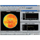
◆ We provide sensor sheets according to the size of the silicon wafer. ◆ We support both batch and single-sheet processing. ◆ The sensor sheets are ultra-thin, with a thickness of approximately 0.1mm, allowing measurements in conditions very close to actual use. ◆ Measurement data can be displayed in 2D and 3D screens. Additionally, the captured data can be replayed, and the analysis functions are comprehensive (please contact us for compatible computer models).
basic information
◆ We prepare sensor sheets according to the size of the silicon wafer. ◆ We support both batch and individual leaf types. ◆ The sensor sheets are ultra-thin, with a thickness of about 0.1mm, allowing measurements in conditions very close to actual use. ◆ Measurement data can be displayed in 2D and 3D screens. Additionally, the captured data can be replayed, and the analysis functions are well-equipped (please contact us for compatible computer models).
Price information
-
Delivery Time
Applications/Examples of results
◆Silicon wafer polishing contact pressure distribution ◆CMP
Recommended products


Distributors

In today's world, where advanced technological capabilities are required of all Japanese companies, we aim to be a trading company that not only embodies "integrity" and "technology," but also explores our customers' needs and responds to their requests, rather than being just a simple trading company.