
Low cost & high imaging quality research atomic force microscope (AFM)
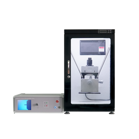
Affordable AFM for laboratories that maintains high image quality without compromise.
This is an atomic force microscope that emphasizes image quality while keeping costs down. - Cost performance that can be considered at less than half the price of conventional models - Supports not only topography but also phase, MFM, LFM, and EFM measurements (some options available) - Adoption of a spring suspension structure reduces noise from vibrations - Easy design for probe replacement and laser alignment - Auto-approach mechanism prevents sample and probe damage during probe descent - Motor-driven step mechanism allows for precise movement to the targeted measurement position - Built-in CCD enables real-time observation and adjustment of the observation position - Modular design makes maintenance and function additions easy It is suitable for improving throughput with multiple units and for being the first AFM in a newly established lab.
basic information
- Model: NanoView-1000 AFM - Operating modes: Contact / Tapping (Options: Contact, Friction, Phase, Magnetic Force, Electric Force) - Maximum sample dimensions: Diameter 90mm, Height 20mm - XY scan range: 20µm (expandable up to 100µm as an option) - Z-axis scan range: 2µm - Resolution: XY direction 0.2nm, Z direction 0.05nm - Stage movement range: ±6.5mm - Number of pixels acquired: 256×256 or 512×512 - Built-in optical system: Magnification 4x, Resolution 2.5µm - Scan speed: 0.6 to 4.34Hz - Control resolution: XY 18bit, Z 16bit (D/A) - Signal acquisition: 14bit A/D, 16bit A/D with simultaneous sampling on two channels - Control method: DSP digital control (sampling 64.0kHz) - Connection interface: USB2.0 - Supported OS: Windows XP / 7 / 8 / 10
Price range
Delivery Time
Model number/Brand name
NanoView-1000 AFM (FSM-Precision Inc.)
Applications/Examples of results
[Observation Examples] - Polystyrene particles (10×10µm) - Fine structure of butterfly wings (20×20µm) - Nanoparticles (3×3µm) - Alumina (10×10µm) - Barium ferrite magnetic materials (12×12µm) - Graphene, carbon nanotubes - DNA, plant-derived proteins - Organic semiconductor deposition films The range of subjects is broad, from inorganic materials to biomolecules, and it is used both as an educational sub-device and for improving throughput through the introduction of multiple units.
Related Videos
catalog(1)
Download All Catalogs
Recommended products
Distributors

Nihon Laser, founded in 1968, is the oldest and largest specialized company in Japan for lasers and optical-related products, having grown alongside advancements in laser technology with the support of our customers as a pioneer in the laser trading industry. We allocate just over 10% of our workforce to engineers, making us a trading company with strong technical expertise. We provide excellent laser products and optical-related products from around the world, including the USA, UK, Germany, France, Switzerland, Denmark, and Lithuania. We have established agency agreements with top-class manufacturers in each country, and currently, we have about 50 overseas trading partners. Additionally, we can independently assemble laser-related equipment sourced from around the world and offer it as application systems. While we are a trading company, we also provide services akin to a fabless manufacturer. With gratitude for our customers' demands, we will continue to offer flexible and aggressive solutions.