
Optical Film Thickness Measurement Device FiDiCa







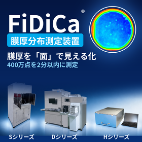
From "point" to "surface" in film thickness measurement. Visualizing film thickness variation with non-contact, high-speed measurement.
FiDiCa is an optical film thickness distribution measurement device that captures thickness as a "surface" rather than a "point." Utilizing a non-contact spectral interference method and a unique analysis algorithm, it rapidly and precisely maps the thickness distribution of semiconductor wafers, films, and liquid films. It acquires data from up to approximately 4 million points with a one-axis line scan, visualizing thickness variations, linear defects, and localized anomalies that are difficult to capture with point measurements. The product line includes the standard S series, the wide-range D series, and the high-resolution H series, allowing selection based on the target and purpose, from thin films to extremely thick films. Models are available from benchtop types to those equipped with CtoC transport systems, supporting the efficiency of measurements and the improvement of quality and yield from research and development to mass production evaluation and inspection.
basic information
■S Series | Standard Model (Note: The following is based on the use of different heads) Measurement film thickness range: Thin film 50nm to 20μm / Thick film 1 to 100μm / Ultra-thick film 20 to 800μm Spatial resolution: Thin film approximately 50 to 150μm / Thick film approximately 80 to 250μm / Ultra-thick film approximately 100 to 300μm ■D Series | Wide Range Model Measurement film thickness range: 50nm to 100μm Spatial resolution: Approximately 5 to 150μm Model with CtoC transport mechanism also available ■H Series | High Resolution Model Measurement film thickness range: 100nm to 10μm Spatial resolution: Approximately 5μm Desktop type / Compatible with full measurement of 6-inch wafers
Price range
Delivery Time
Applications/Examples of results
It can be widely used from research and development of semiconductors, semiconductor materials, and electronic components, to quality evaluation of films and glass, and thickness inspection in mass production processes. For thin films, it evaluates thickness distribution and coating irregularities of SiO₂ films, sputtered films, resist films, liquid films, oil films, and coated films. For thick and ultra-thick films, it measures thickness distribution of various wafers, films, bulk wafers, and glass. By mapping the entire surface, it helps identify local thickness anomalies and line defects, supporting the examination of film formation and coating conditions, process improvement, and quality control. The H series is suitable for high-resolution thickness distribution measurement on device patterns, while the D series with CtoC transport is suitable for continuous evaluation on mass production lines. You can consult us for model selection based on your needs.
catalog(1)
Download All Catalogs
Recommended products


Distributors

In this department, we provide total solutions for assembly by offering a diverse range of products and high technical capabilities to meet the challenges of our customers, who are globally expanding primarily in China, Thailand, Malaysia, and Vietnam. We focus on excellent assembly equipment from Panasonic Connect (formerly Panasonic Smart Factory Solutions) to support high performance, miniaturization, and lightweight electronics products, as well as peripheral equipment, technical support, and maintenance. Please take a look at our introduction video. https://www.youtube.com/watch?v=efdEd2BVT-A