High-performance Single-wafer Processing Atmospheric Pressure CVD (APCVD) System (A200V)

Small quantities and wide varieties. NSG(SiO2)/PSG/BPSG deposition. Single-wafer processing atmospheric pressure CVD (APCVD) system (Compatible with 8-inch SiC wafers)
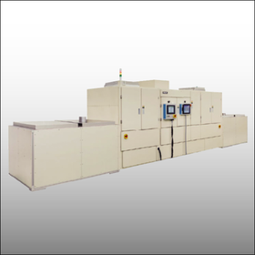
A200V is a single-wafer processing atmospheric pressure CVD system (APCVD system) for silicon oxide (SiO2) deposition, such as interlayer insulating deposition, passivation deposition (protective deposition), and sacrificial deposition. 【Features】 ・Ideal for insulating depositions and diffusion/plasma mask depositions. ・Low particle film deposition by single-wafer face-down deposition. ・High safety and deposition stability by using a sealed chamber. ・Wafer warp correction function (patented) for SiC wafers. ・Low-load, long-cycle maintenance. ・Compact cabinet and adjacent installation to the mirror type for space saving. ・Low CoO (low running cost) 【Applications】 ・Interlayer dielectric deposition for power semiconductors (NSG/PSG/BPSG) ・Hard mask for diffusion/ion implantation, Sacrificial depositions (NSG) ・Passivation depositions (protective depositions, insulating depositions) (NSG) ・Optical Waveguide (NSG/BPSG) *For more details, please contact us or download the catalog for further information.
basic information
The face-down deposition method, in which the wafer is heated in a sealed chamber with the deposition surface facing down, the back side adsorbed, and the process gas is blown up from the bottom, achieves safe, high-quality deposition with low particle counts. The patented wafer warpage correction function enables reliable adsorption of wafers with large warpage, such as SiC wafers, to achieve excellent film thickness uniformity. The composition reducing the adhesion of side reaction products around the wafer improves maintainability (low load and long cycle time). The compact cabinet size allows adjacent installation to minimize the footprint. ●Equipment size (mm): 890(W) x 2300(D) x 2250(H) ●Gas type: SiH4/O2 (SiH4/PH3/B2H6/O2/N2) TEOS/O3 (TEOS/TMOP/TEB/O3/O2/N2) (optional) ●Deposition temperature: 350~450 degrees. *For more details, please contact us or download the catalog to view.
Price range
Delivery Time
Model number/Brand name
A200V
Applications/Examples of results
【Applications】 ・Interlayer dielectric for power semiconductors (NSG/PSG/BPSG) ・Hard mask for diffusion/implanter, Sacrificial deposition (NSG) ・Passivation deposition (protective deposition, insulating deposition) (NSG) ・Optical Waveguide (NSG/BPSG) 【Delivery Record】 ・Domestic and foreign semiconductor device manufacturers. ・Universities, research institutes, and research laboratories.
catalog(1)
Download All Catalogs
Recommended products


Distributors

Founded in 1930 as a specialized trading company for imports and exports, we celebrated our 90th anniversary in 2020 and are fully committed to the further development of the M.WATANABE Group. Since the mid-1960s, we have started manufacturing and selling our own products such as quartz processed products, silicone rubber molded products, and cleaning equipment, under the policy of selling silicon (Si) related products to the semiconductor industry. As a manufacturing trading company, we have grown alongside the IT society by providing high-quality products and services. Moving forward, we aim to create a company where employees of the group companies, centered around M.WATANABE & CO.,LTD., work vibrantly every day, and the entire workplace becomes a learning organization. We are determined to continue striving in all our business endeavors with a strong will to respond to the true needs of society. We sincerely ask for your continued support and patronage.