
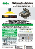
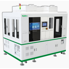
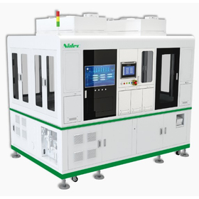
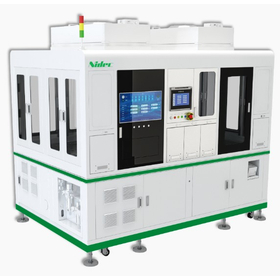
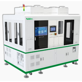
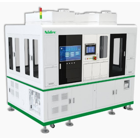
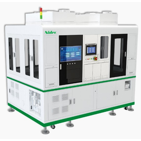
TGV Through Hole Glass Substrate Inspection Device
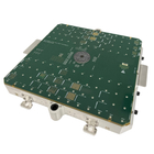
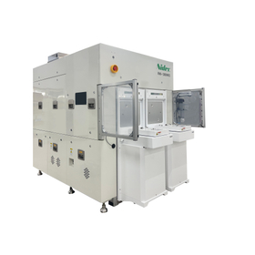
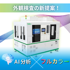
The optimal imaging inspection device for TGV inspection has been completed!
By using high-resolution 2D and 3D cameras, and combining them with NIR (near-infrared), we have achieved the detection of all types of defects. In addition to conventional high-precision surface inspection, it is now possible to measure internal defects and depth using NIR. Furthermore, the range of compatible materials has expanded beyond just glass to include SiC/silicon wafers, ABF films, and more. Please feel free to contact us.
basic information
For more details, please download the materials or feel free to contact us.
Price range
Delivery Time
Applications/Examples of results
For more details, please download the materials or feel free to contact us.
catalog(4)
Download All Catalogs

Recommended products
Distributors

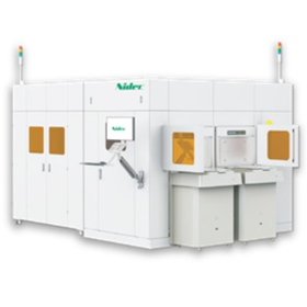
Our inspection target areas include printed circuit boards, semiconductor packages, and display panels. These are core components of information and communication devices that are growing increasingly due to advancements in IT, as well as widely adopted digital home appliances. Printed circuit boards, semiconductor packages, and display panels are evolving at an astonishing speed, and higher precision technologies are required in inspections. Our company holds a significant share in these inspection fields that demand cutting-edge technology, and we have delivered numerous products recognized as "de facto standards" in the industry worldwide.