Sputtering device


Combination of CVD chamber, deposition chamber, plasma cleaning chamber, etc. is also available! Many custom manufacturing achievements!
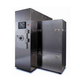
We would like to introduce the "sputtering equipment" handled by Japan Create. We offer a range of products including the "load-lock type sputtering equipment" equipped with our unique sputter cathode, as well as "multi-target sputtering equipment" and "sputtering equipment for three-dimensional objects." We also have a track record of custom-made equipment such as ultra-high temperature sputtering systems for thin-film MEMS, IBS systems for research and development, and sputtering equipment with GB for organic EL. Please feel free to contact us when you need assistance. 【Features of Load-Lock Type Sputtering Equipment】 ■ Compatible with moving magnets, allowing for full-area erosion ■ Equipped with our unique rapid heating mechanism for substrates, achieving a substrate temperature of 900°C ■ Enables high-speed and stable reactive sputter deposition ■ Capable of low-temperature processes such as lift-off ■ Tray transport is also supported *For more details, please refer to the PDF document or feel free to contact us.
basic information
【Lineup】 ■ Load-lock type sputtering system ■ Multi-target sputtering system ■ Sputtering system for three-dimensional objects *For more details, please refer to the PDF document or feel free to contact us.
Price range
Delivery Time
Applications/Examples of results
【Custom Manufacturing Achievements (Excerpt)】 ■ Ultra-high temperature sputtering equipment for thin film MEMS ■ Batch-type multi-target sputtering equipment ■ Batch-type sputtering equipment for thin film MEMS ■ IBS equipment for research and development ■ Composite film deposition equipment for MEMS ■ Multi-target composite sputtering equipment ■ Sputtering equipment with GB for organic EL, etc. *For more details, please refer to the PDF document or feel free to contact us.
catalog(1)
Download All Catalogs
Recommended products


Distributors

Japan Create has been challenging cutting-edge technologies to respond to the diversification of the semiconductor industry with high precision, labor-saving, and miniaturization. We seek infinite possibilities in high technology and create reliable know-how that matches user needs with our uniqueness. We will continue to strive towards high-level technology.