High-Rate Deposition. Piezoelectric Film Formation Sputtering Device

For semiconductors, MEMS, electronic components, etc.! High-speed and stable continuous film deposition is possible from single crystal epitaxial buffer layers to piezoelectric films!
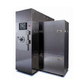
The "Piezoelectric Film Formation Sputtering Device" is a product capable of detecting elements that contribute to the reduction of piezoelectric properties, thanks to the incorporation of a plasma emission monitor. It allows for continuous film formation from a single crystal epitaxial buffer layer to the piezoelectric film. Additionally, high-speed and stable reactive sputter deposition is possible through plasma analysis and feedback control using a luminescence analysis system. Equipped with our unique rapid temperature rise and fall substrate heating mechanism, it achieves a substrate temperature of 900°C. 【Features】 ■ Deposition structure that maximizes the axis length contributing to piezoelectricity ■ Equipped with our proprietary sputter cathode ■ Compatible with moving magnets, allowing for full-area erosion ■ Tray transport compatibility ■ Combinations with CVD chambers, deposition chambers, plasma cleaning chambers, etc., are also supported *For more details, please refer to the PDF document or feel free to contact us.
basic information
【Specifications (Excerpt)】 ■Substrate Size: Maximum φ12 inches ■Sputter Cathode: Magnetron type, target shutter ■Sputter Power Supply: RF or DC ■Process Gases: Ar, O2, N2, others ■Substrate Stage ・Substrate Heating: 700℃ (substrate surface) ・Rotation: Up to 20 rpm ■Vacuum Exhaust ・Configuration 1: TMP + DP ・Configuration 2: CP + DP ■Pressure Control: APC control *For more details, please refer to the PDF document or feel free to contact us.
Price range
Delivery Time
Applications/Examples of results
【Applications】 ■Semiconductors ■MEMS ■Electronic components ■Optical components ■Automotive components *For more details, please refer to the PDF document or feel free to contact us.
catalog(1)
Download All Catalogs
Recommended products


Distributors

Japan Create has been challenging cutting-edge technologies to respond to the diversification of the semiconductor industry with high precision, labor-saving, and miniaturization. We seek infinite possibilities in high technology and create reliable know-how that matches user needs with our uniqueness. We will continue to strive towards high-level technology.