High-Rate Depo. Piezoelectric Film Formation Sputtering Device


For semiconductors, MEMS, electronic components, etc.! High-speed and stable continuous film deposition is possible from single crystal epitaxial buffer layers to piezoelectric films!
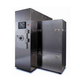
The "piezoelectric film formation sputtering device" is a product that enables continuous film formation from a single crystal epitaxial buffer layer to a piezoelectric film. Through plasma analysis and feedback control using a plasma emission monitor, it allows for fast and stable reactive sputtering, as well as the detection of elements that contribute to the degradation of piezoelectric properties. It is equipped with our unique rapid heating and cooling substrate heating mechanism, achieving a substrate temperature of 900°C. *For more details, please refer to the PDF materials or feel free to contact us.
basic information
【Features】 ■ Deposition structure that maximizes the length of the axis contributing to piezoelectricity ■ Equipped with our proprietary sputter cathode ■ Compatible with moving magnets, allowing for full erosion ■ Tray transport is also supported ■ Combinations of CVD chamber, deposition chamber, plasma cleaning chamber, etc., are also supported We also handle other wet process equipment and vacuum process equipment, so please take a look. "Oxide/Nitride Plasma CVD Equipment" ■ Achieves low stress, high hardness, and high insulation through a two-frequency independent printing method ■ Realizes excellent film thickness distribution and reproducibility "Carbon Nanotube Synthesis Equipment" ■ Fully automatic CNT synthesis is possible ■ Achieves excellent substrate temperature distribution and gas flow method ■ Equipped with a substrate plasma cleaning system ■ Realizes excellent film thickness distribution and reproducibility * For more details, please refer to the materials. Feel free to contact us with any inquiries.
Price range
Delivery Time
Applications/Examples of results
*For more details, please refer to the materials. Feel free to contact us as well.*
catalog(30)
Download All Catalogs


Recommended products


Distributors

Japan Create has been challenging cutting-edge technologies to respond to the diversification of the semiconductor industry with high precision, labor-saving, and miniaturization. We seek infinite possibilities in high technology and create reliable know-how that matches user needs with our uniqueness. We will continue to strive towards high-level technology.