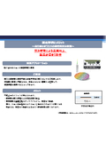
Optical area scanner "Flying Spot Scanner"
High-speed area scanning unaffected by vibrations. For online, offline, quality control, and wafer inspection applications.
The "Flying Spot Scanner" is an optical measuring device that can perform wide-area scans (up to φ80) using XY2-axis galvanometer mirrors. Since stage scanning is not required, there is no influence from vibrations of the stage. Thanks to the principle of spectral interference, it can measure thickness, dimensional shapes, and inspect surface defects. Additionally, because the incident and reflected light are in a coaxial optical system, good results can be obtained even on glossy surfaces. 【Features】 ■ Wide-area scanning ~φ80mm ■ High resolution XY 6.5μm~, Z 1nm~ Minimum beam spot diameter 13μm, high Z resolution due to spectral interference method ■ No XY stage required, no stage vibrations Area scanning using galvanometer mirrors ■ Reduced development costs and shortened development lead times Software development kit (DLL, etc.) available for device integration ■ Applications Thickness measurement of glass substrates for FPD and LCD, measurement of wafer warp (distortion), lens shape inspection, PCB board shape inspection, height measurement of small precision parts, etc. *For more details, please refer to the materials. Feel free to contact us with any inquiries.
basic information
【Semiconductor Applications】 ■ High-speed BGA Measurement ■ High-speed Substrate Inspection ■ High-speed Wafer Thickness Measurement ■ High-speed Warpage Measurement *For more details, please refer to the PDF document or feel free to contact us.
Price range
Delivery Time
Applications/Examples of results
[Keywords: Applications, Measurement Items, Benefits, etc.] Non-contact sensors, optical sensors, spectroscopic interference method, thickness, thin films, thick films, gaps, height, flatness, TTV (Total Thickness Variation), shape, measurement, inspection, high speed, 3D, area scan, full surface, high precision, inline, monitoring, in-situ, during processing, before and after processing, polishing, offline, standalone machines, tabletop machines, sampling, embedded, semiconductors, wafers, wafer bonding, Si wafers, Si, GaAs, InP, SiC, LiNbO3 (LN), LiTaO3 (LT), GaN, SiP, Al2O3 (sapphire), weld joints, glass, PCB, coating, films, multilayer films, applied films, conformal coating, electrode layer coating, stent coating, polyimide, PVB, resin materials, flux, adhesives, insulating films, air layers, transparent, transparent bodies, gloss, mirror finish, simple.
Related Videos
catalog(8)
Download All Catalogs


News about this product(1)
Recommended products
Distributors
Presitech is a specialist in laser material processing and optical measurement technology. We are not just a supplier of systems and components, but a professional partner in ensuring a smooth processing process for our customers. We offer consultations from the foundational stage and accurately consult with customers on their requests and objectives. We understand that the key to success in unique processing processes lies in the four components of exhibition, monitoring, processing, and control. Only by doing so can we provide appropriate solutions for our customers' applications. Our high-quality products, such as laser processing heads, quality monitoring systems, and optical measurement systems for spacing/thickness measurement, allow customers to directly benefit from our decades of experience. Our optical sensors are characterized by the highest precision and dynamic adaptability. Furthermore, they detect accurate values even in high-speed measurements.


