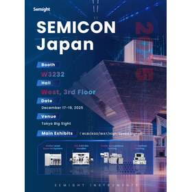
Power Device "Wafer-Level Burn-In"
Protect each circuit with complete hardware! Supports simultaneous burn-in of up to 6 wafers.
"Wafer level burn-in" is equipment that allows for burn-in testing of GaN and SiC devices at the wafer level, significantly reducing the inspection loss of power modules. It can accommodate simultaneous burn-in of up to 6 wafers. Additionally, independent burn-in condition settings are possible for each fixture. Complete hardware protects each circuit. 【Features】 - Suitable for burn-in of GaN and SiC wafers - Independent burn-in condition settings for each fixture - Allows simultaneous power-on and burn-in of all chips on the wafer - HTGB voltage ±75V, HTRB voltage 2000V (upgradeable) - Supports Igss, Idss, Vth, Idson testing - Temperature range RT-200C *For more details, please refer to the PDF document or feel free to contact us.
basic information
Parameter Specification Applicable Products GaN, SiC Wafer Applicable Packaging 4-inch, 6-inch Wafer Burn-in Parameters HTGB, HTRB Test Parameters Igss, Idss, Vth System Size (mm) 2100(W) X 1900(H) X 1800(D) System Power Consumption <32 kW Nitrogen Protection >0.6 mPa Temperature Range Room Temperature - 175 ℃ Voltage Range Gate ±75 V, Source 2000 V System Channels 720 System Layers 6 layers Current/Voltage Overshoot No overshoot in any case MES Docking Compatible with MES docking *For more details, please refer to the PDF document or feel free to contact us.
Price range
Delivery Time
Applications/Examples of results
For more details, please refer to the PDF document or feel free to contact us.
catalog(1)
Download All CatalogsRecommended products
Distributors
We are a global supplier of advanced testing and measurement equipment. We provide high-performance and highly integrated measurement solutions that can support everything from research and development to mass production processes in cutting-edge fields such as high-speed communication, optical chips, electronic measurement, and power semiconductors. Since our founding, we have placed "Dedication and Craftsmanship" at the core of our corporate values, pursuing product development that combines deep insights into measurement principles with a spirit of craftsmanship. Aiming to be "the best testing solution company supporting global technological innovation," we will continue to provide high-performance, high-efficiency, and highly reliable solutions to address global industrial challenges.


