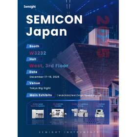
CT8201 LD chip compatible normal temperature and high temperature die tester
One unit compatible with LIV·EA·spectrum — fully automatic, ultra-high efficiency tester, essential for mass production.
The Semight RT & HT Daitester CT8201 is a high-performance automatic test system capable of performing LIV scans, EA scans, and spectral scans for DFB lasers and EML (Electro-absorption Modulated Laser) devices at both room temperature and high temperature in two temperature ranges. ■ Main Supported Tests and Functions - Forward and reverse optical measurements (photocurrent/IV measurements) - Forward spectral measurements (emission spectrum) - Simultaneous support for two temperature zones (parallel measurement of room temperature and high temperature on two independent platforms) - Equipped with high-precision thermal control and stable supply probe structure ■ Productivity, Accuracy, and Stability The CT8201 can complete all six processes (loading, transport, recognition, measurement, classification) in just 6 seconds. Particularly in EML measurements, further throughput optimization is possible depending on the measurement item configuration. Additionally, it incorporates an eccentric cam structure, high-precision linear motors, high reproducibility stepping control, high thermal conductivity chuck, and high rigidity probe structure, achieving ultra-high precision and ultra-high stability, making it ideal for die sorting and reliability testing in mass production.
basic information
▶Supported devices: Semiconductor laser chips (DFB, EML) ▶Supported test items: LIV scan, EA scan, spectral scan ▶Temperature zones: Two-zone configuration of room temperature zone / high temperature zone ▶Temperature range: Room temperature to a maximum of approximately 85°C (customizable according to specifications) ▶Processing time per chip: Fastest within 6 seconds (varies depending on EML measurement items) ▶Configuration units: Wafer supply section, chip transport section, position correction section, OCR reading section, test section, chip storage section ▶Supported processes: Wafer loading, chip transport, ID/OCR reading, room temperature/high temperature testing, discharge/sorting ▶Optical measurement: Forward and reverse photoelectric measurement, spectral measurement ▶Transport accuracy: High-precision linear motor + eccentric cam structure ▶Electrical connection: High-stability current-probing, high thermal conductivity stage ▶Sorting function: Automatic classification based on pass/fail judgment ▶Maintenance: Individual return and maintenance possible for each mechanical module ▶User interface: Fully automatic alarm notification, flexible pass/fail condition and measurement plan settings available
Price range
Delivery Time
Applications/Examples of results
Evaluation and implementation are already underway with top-class companies in the industry, and they are actively adopting our solutions.
Detailed information
-

▶Fully Automated, Intelligent Integrated Solution A highly integrated fully automated test system that fully covers the complex chip inspection process.
-

▶ Loading Module This module consists of the following four sub-functional modules: - Chimple Z-axis Module - X/Y-axis Movement Module - Blue Film Rotation Module - Pickup Function Unit This automates a series of processes for high-precision adsorption and transfer of chips on a wafer or an extension ring.
-

▶High Temperature and Normal Temperature Test Module This module is a high-precision test unit compatible with two temperature ranges, consisting of the following components: - Hollow-type rotating platform (supports wafer flipping and transport switching) - Two 3-axis chip alignment modules positioned at the front and back - 3-axis optical detection module (PD and collimator optical system) - ID and position recognition camera installed on the top - Power-on Probe module: Executes position and angle correction after transport, allowing for accurate power-on and measurement of the chip The PD (photodiode) and collimator can be switched at high speed using independent drive axes, supporting automatic switching of functions according to the measurement mode.
-

▶Camera & Power Probe Module This module is composed as a composite unit for chip position recognition, ID identification, and power measurement. 【Camera System Configuration】 - Loading Camera (right side of the device): It performs chip recognition and seating determination during chip transport. It can flexibly collaborate with different functional modules depending on the incoming form. - High-Temperature/Room Temperature Test Module Upper Camera (central part of the device): After chip transport, it captures images from multiple angles using a 3-axis movement module, performing high-precision alignment correction of the chip position. In the high-temperature zone, ID recognition is also executed simultaneously. 【Probe Power Module】 - Each test platform can accommodate up to three sets of power probes. - A configuration with PD (Photodiode) + backlight can be added as an option. - Depending on the type of chip, LIV measurement, extinction ratio measurement, etc., can be flexibly configured. This module provides an environment for one-touch continuous measurement of optical parameters for DFB/EML products, achieving improved yield and process efficiency in mass production sites.
-

▶ Blanking Binning Module This module has four tray installation areas and is compatible with 4-inch and 6-inch blue tape. Additionally, customization of the corresponding unloading carrier is possible according to customer requests.
Line up(2)
| Model number | overview |
|---|---|
| CT8201 | Supports LIV scan / EA scan / spectral scan measurements of the optoelectronic characteristics of DFB or EML lasers at room temperature and high temperature (25℃ to 95℃) |
| CT8202 | Capable of conducting LIV scan and spectral scan measurements of the optoelectronic characteristics of semiconductor lasers at low temperature / room temperature / high temperature (-40℃ to 95℃) |
catalog(2)
Download All CatalogsRecommended products
Distributors
We are a global supplier of advanced testing and measurement equipment. We provide high-performance and highly integrated measurement solutions that can support everything from research and development to mass production processes in cutting-edge fields such as high-speed communication, optical chips, electronic measurement, and power semiconductors. Since our founding, we have placed "Dedication and Craftsmanship" at the core of our corporate values, pursuing product development that combines deep insights into measurement principles with a spirit of craftsmanship. Aiming to be "the best testing solution company supporting global technological innovation," we will continue to provide high-performance, high-efficiency, and highly reliable solutions to address global industrial challenges.


