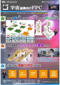
High-frequency compatible flexible substrate (MPI specification)


Supports low transmission loss and impedance matching! There are various applications such as mobile electronic devices and IoT devices.
The "High-Frequency Compatible FPC (MPI Specification)" is a product designed to support low transmission loss and impedance matching. 〇 It has excellent heat resistance and can accommodate solder mounting and bonding. 〇 It allows for high flexibility in processing, similar to standard polyimide. ● FPC high-frequency analysis service (optional) It can be used for various applications. 【Examples of Applications】 ■ Mobile electronic devices such as smartphones ■ Optical communication modules ■ IoT devices ■ Video equipment (4K/8K) ■ Other alternatives to coaxial cables #Flex #FPC #FlexibleCircuitBoard #FlexiblePrintedCircuitBoard #CircuitBoard #PrintedCircuitBoard #HighFrequency #Impedance #ShortLeadTime #MassProduction
basic information
For more details, please refer to the PDF document or feel free to contact us.
Price range
Delivery Time
Applications/Examples of results
For more details, please refer to the PDF document or feel free to contact us.
catalog(14)
Download All Catalogs


News about this product(5)
-

[Press Release from Taiyo Techno Rex] Announcement regarding the launch of electronic device contract manufacturing services.
We have newly launched an "Electronics Manufacturing Services (EMS)" that provides a comprehensive response from material procurement, circuit design, manufacturing, and assembly to functional testing and shipping in the traditional FPC (Flexible Printed Circuit Board) manufacturing process. In recent years, the use of FPCs has expanded across various fields such as medical devices and industrial equipment, leading to an increased demand not only for supply but also for a one-stop solution that encompasses circuit design, module manufacturing, and even final product assembly. To meet these market demands, we have strengthened our collaboration with electronics manufacturing companies and established a manufacturing system that covers everything from material procurement to assembly. With this service, customers can reduce interactions with multiple vendors, achieve shorter lead times, and improve manufacturing efficiency. Our stringent quality control system ensures the delivery of highly reliable products. The product areas we can support include automotive devices, medical devices, industrial equipment, robotics, communication devices, lighting equipment, and home appliances, allowing us to meet a wide range of manufacturing needs.
-
[Press Release from Taiyo TechnoRex] Regarding the Improvement of High-Density Wiring Formation Technology Using the Patterned Beer Fill Method
Our company has further improved the technology for forming high-density wiring in our core business of electronic substrates, specifically in flexible printed circuit boards (FPCs). In recent years, electronic devices such as medical equipment and industrial machinery have been advancing in miniaturization and lightweight design. To incorporate many functions into limited space, there is a demand for increased wiring density on the substrate. Therefore, we have been working on establishing filled via technology and improving the M-SAP method. The filled via structure involves filling vias (holes) made by laser in the insulating layer with copper plating, ensuring electrical connections on both sides of the substrate while reducing the recesses of the vias, which allows for component mounting on the vias and leads to high-density mounting. On the other hand, the M-SAP method significantly improves line width management by laminating copper to form circuits, enabling high-density wiring. This time, based on the pattern via fill method that leverages these characteristics, we successfully formed wiring with a pitch of 30μm on a double-sided substrate with a filled via structure. We will continue to aim for further improvements in high-density wiring formation technology through ongoing development, prototyping, and verification.
-
Press Release from Taiyo TechnoRex: Participation in Wakayama Prefecture's "Space Town Development Promotion Project"
Our company has decided to participate in the "Space Town Development Promotion Project (Kii Space HUB)," which aims to create new industries and revitalize the region with a space theme, promoted by Wakayama Prefecture, in our core business of electronic substrate. Taking this opportunity, we will actively advance our technological development and business enhancement in the space field. The Space Town Development Promotion Project is a project aimed at the accumulation of the space industry, human resource development, and regional revitalization in Wakayama Prefecture, where the private rocket launch site "Spaceport Kii" is located, and it has garnered national attention. We aim to contribute to the lightweight and high functionality of space equipment by leveraging the manufacturing technologies of flexible printed circuit boards and electroforming that we have cultivated so far. In the future, we will actively engage in human resource development for those involved in the space business, starting with the provision of technology for satellite-mounted equipment and communication modules. We will also consider collaboration with private space companies, promoting value creation and business development in this new field of the space industry, while striving to balance technological innovation and social contribution, and continuing our challenges toward realizing a sustainable future.
-

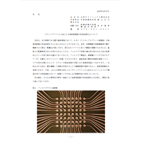
【TTL_Exhibition Participation Information】JPCAShow2025 'Newly Developed Topics.'
◆FPC (Flexible Printed Circuit Board)◆ ~Tayo Technorex's Strengths in the FPC Manufacturing Process~ The manufacturing of FPC requires multiple critical processing steps. Improving the "strengths" of each process directly leads to advancements in technology and quality, as well as new product development. This time, we will introduce the "strengths" we have cultivated over many years in each process! <Design> Circuit design, artwork, S-parameter analysis <Layer Connection> Build-up FPC, filled vias, small-diameter vias <Circuit Formation> MSAP method, thin copper, thick copper <Insulation Treatment> High-precision openings ±20μm, LCP coverlay <Surface Treatment> Standard NiAu to special plating options (Ni-Pd-Au, direct Au, etc.) <Post-Processing> High-precision outline processing ±50μm, diverse tools <Assembly> Solder mounting, ACF bonding, wire bonding, ultrasonic joining, EMS support ◆Various Substrates and Ceramic Material Systems◆ Introduction of AI technology, final appearance inspection equipment, and electrical testing equipment ◆Efficiency and Automation◆ Proposals for utilizing FA and collaborative robots
-

【TAIYO】FPC Manufacturing Technology: "Announcement Regarding the Development of All-Polyimide Build-Up Substrates"
Our company is working on the development of build-up substrates using polyimide for the insulating layer, aimed at miniaturizing, thinning, and lightening multilayer substrates in our core electronic substrate business. We are pleased to announce that we have established the core filled via technology. In electronic devices that are becoming lighter, more compact, and high-functioning, substrates (build-up substrates) capable of high-density wiring and high-density mounting are in demand. However, typically, the core layer of build-up substrates uses rigid boards, which increases the thickness of the substrate and hinders the lightweight and compact design of electronic devices. The filled via technology we have established involves filling holes (vias) made by laser in flexible printed circuit boards (FPC) with an insulating layer of polyimide with copper, and flattening the surface of the filled areas. By using this FPC as the core layer or outer layer of build-up substrates, it becomes possible to achieve both high-density wiring and high-density mounting along with thinning. We plan to start providing build-up substrates using this technology within the fiscal year 2022, and furthermore, by applying this technology to our strength in high-frequency compatible FPCs, we will respond to the demand for miniaturization of communication devices.
Recommended products


Distributors

Taiyo TechnoRex Co., Ltd. continues to operate in the fields of prototype development of flexible printed circuit boards (FPC) and printed circuit board testing systems. Since FPC is fundamentally related to the structure of hardware, both high precision quality and shortened development time are required. We have extensive experience and know-how in the manufacturing processes of single-sided FPC, double-sided FPC, multilayer FPC, and their advanced types, and we continuously improve and enhance our technology, resulting in consistent evaluations of our delivery times and quality. Additionally, while technically advancing further miniaturization and high density, we are also undertaking new initiatives such as bump-type and special material electroplating. On the other hand, our printed circuit board testing systems mainly consist of electrical inspection systems and final appearance inspection systems, which are adopted in the mass production sites of FPCs and package/module-type substrates. They operate day and night in quality control settings for substrates used in smartphones, automotive applications, and various electronic devices. We will continue to respond to the increasingly diverse market needs. *On December 21, 2023, the company name was changed from "Taiyo Kogyo Co., Ltd." to "Taiyo TechnoRex Co., Ltd."*