Collaboration with boundary scan testing using a flying probe tester.


We will create new value through the mutual complementarity of ICT and BST.
In-circuit testing with a flying probe tester excels at inspecting the electrical characteristics of implemented electronic components in analog circuits. However, components that cannot be probed make electrical testing difficult, and functional testing of digital circuits is challenging. On the other hand, boundary scan testing allows for quick interconnection testing between LSI pins and on-board programming for FPGAs, but it can only test digital circuits around ICs that comply with the boundary scan standard, and it also requires specialized fixtures for connections. At Takaya Corporation, we possess technology that uses flying probes instead of fixtures to connect 4 to 5 scan-compatible pins and measuring instruments required for boundary scan testing. This allows for boundary scan testing even when the counterpart of a boundary scan-compliant IC is a non-boundary scan-compliant IC or passive components (such as connectors) by enabling the flying probe to function as a virtual boundary scan cell. With a single flying probe tester, it is possible to conduct comprehensive testing of both digital and analog circuits, thereby significantly enhancing testing efficiency compared to before.
basic information
Please contact the sales representative.
Price range
Delivery Time
Applications/Examples of results
Benefits arising from mutual complementation - Significant improvement in test coverage - Improved test throughput - Possible reduction in implementation area of digital circuit domains in board design (TP reduction) - More accurate fault diagnosis - Onboard programming or FPGA writing is possible
Related Videos
catalog(8)
Download All Catalogs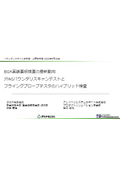


News about this product(15)
-

We will exhibit a corporate booth at the 39th Spring Conference of the Electronics Packaging Society. (Takushoku University, Bunkyo Campus)
Takaya Corporation will exhibit a corporate booth at the 39th Electronics Packaging Society Spring Conference, which will be held from March 11 (Tuesday) to March 13 (Thursday), 2025, at the Bunkyo Campus of Takushoku University. This conference is held annually under the management of the Japan Electronics Packaging Society, providing a platform for the presentation and exchange of the latest research and development results related to electronics packaging technology. Starting in 2023, a hybrid format combining in-person participation and online attendance has been implemented, attracting around 700 participants, primarily from academia and industry related to electronics packaging technology. When you visit, please be sure to stop by Takaya's booth. (Registration and payment of participation fees are required for attendance.)
-

I participated in the 29th Okayama Research Park Research and Exhibition Presentation and conducted a panel exhibition.
On December 17th (Tuesday), we participated in the research and exhibition presentation held at Okayama Research Park and conducted a panel display. We had the opportunity to interact with representatives from companies, universities, and technical colleges in the prefecture. The presentation panels from each organization can be viewed on the Okayama Research Park Research and Exhibition Presentation website.
-

We will be exhibiting a poster at the 29th Okayama Research Park Research and Exhibition Presentation.
The "29th Okayama Research Park Research and Exhibition Presentation" will be held with the aim of presenting and disseminating research results from companies and institutions related to the "Okayama Research Park." We will have a poster exhibition on "Latest Trends in Hybrid Testing Systems Combining JTAG Testing and Flying Probe Testers." We invite companies, universities, and institutions interested in industry-academia-government collaboration to participate freely. Poster exhibition on research seeds (Industry-Academia Collaboration Model Booth + 8 fields) 《Fields》 ○ Precision Processing and Machinery ○ Materials Technology ○ Semiconductors ○ AI, IoT, Robotics ○ Medical, Bio, Food ○ Environment, Chemistry, Energy ○ Measurement, Inspection ○ Others ■ Organized by Okayama Prefecture, Okayama Prefectural Industrial Promotion Foundation ■ Supported by Okayama University, Okayama Prefectural University, Okayama University of Science, Kibi International University, Kawasaki Medical University, Kawasaki University of Medical Welfare, Shujitsu University and Shujitsu Junior College, Notre Dame Seishin University, Tsuyama National College of Technology, China Vocational Ability Development University, IPU International Pacific University, Okayama Research Park Incubation Center (ORIC)
-

I received the Excellent Award at the 38th Electronics Packaging Society Spring Conference.
From March 13 (Wednesday) to 15 (Friday), 2024, at the "38th Spring Conference of the Electronics Packaging Society" held at Tokyo University of Science, Takaya Corporation presented a lecture titled "Latest Trends in Hybrid Testing Systems Combining JTAG Inspection and Flying Probe Testers," which received the Excellence Award at the conference. On September 12, 2024, a ceremony was held at Daido University in Aichi Prefecture during the "MES2024 Symposium," where we were presented with a commemorative plaque.
-

MES2024 34th Microelectronics Symposium Exhibition Booth Participation Information
Takaya Corporation will exhibit a corporate booth at the "MES024 34th Microelectronics Symposium," which will be held from September 11 (Wednesday) to 13 (Friday), 2024, at the Daido University Takiharu Campus in Minami Ward, Nagoya City. When you visit the symposium, please be sure to stop by Takaya's booth. Organizing Office (The Japan Society of Electronics Packaging) 167-0042 Tokyo, Suginami Ward, Nishiogikita 3-12-2 TEL: 03-5310-2010 For details and the latest information, please refer to the related materials flyer and the MES2024 website.
Recommended products


Distributors

Founded in 1894 as a textile company, Takaya Textile expanded and established its electronics division in 1966, beginning the assembly of transistor radios. Currently, in addition to contract manufacturing services (EMS) related to electronic devices, the company actively manufactures and sells in-circuit testers (printed circuit board inspection devices), RFID-related equipment (technology that enables information exchange through short-range wireless communication from IC information tags), and engages in IT consulting and system solutions, among various electronics businesses both domestically and internationally. We will continue to evolve as a corporate group that contributes to the development of society, with textiles and electronics as our two pillars.