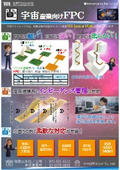
Bump FPC


A bump with a minimum diameter of Φ20µm is formed at the terminal section of the FPC. The bump is used as a contact point and is applied in high-precision circuit testing, etc. (Flexible substrate)
The bump FPC is a bump generation technology that our company specializes in, applied to the FPC. It is optimal for testing fine-pitch insertion terminals and display lighting tests when combined with our contact clips and hand presses. *For more details, please refer to the PDF document or feel free to contact us. #Flexible #FPC #FlexibleCircuitBoard #FlexiblePrintedCircuitBoard #CircuitBoard #PrintedCircuitBoard #Special #Bump #ShortLeadTime #MassProduction
basic information
Flexible printed circuit board Flexible substrate
Price range
Delivery Time
Applications/Examples of results
For more details, please refer to the PDF document or feel free to contact us.
catalog(11)
Download All Catalogs


News about this product(3)
-
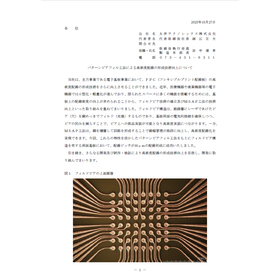
[Press Release from Taiyo TechnoRex] Regarding the Improvement of High-Density Wiring Formation Technology Using the Patterned Beer Fill Method
Our company has further improved the technology for forming high-density wiring in our core business of electronic substrates, specifically in flexible printed circuit boards (FPCs). In recent years, electronic devices such as medical equipment and industrial machinery have been advancing in miniaturization and lightweight design. To incorporate many functions into limited space, there is a demand for increased wiring density on the substrate. Therefore, we have been working on establishing filled via technology and improving the M-SAP method. The filled via structure involves filling vias (holes) made by laser in the insulating layer with copper plating, ensuring electrical connections on both sides of the substrate while reducing the recesses of the vias, which allows for component mounting on the vias and leads to high-density mounting. On the other hand, the M-SAP method significantly improves line width management by laminating copper to form circuits, enabling high-density wiring. This time, based on the pattern via fill method that leverages these characteristics, we successfully formed wiring with a pitch of 30μm on a double-sided substrate with a filled via structure. We will continue to aim for further improvements in high-density wiring formation technology through ongoing development, prototyping, and verification.
-

【TTL】Microfabrication technology! Applying techniques such as electroplating, silicon etching, and glass etching to the development of various advanced technologies!
Microfabrication technology (photofabrication) plays an important role as a production technology, producing precision machined components such as lead frames, HDD suspensions, encoders, TAB tapes, various filters, and decorative items. Additionally, based on photofabrication technology, current advanced technologies such as printed circuit boards, photomasks for LSI, color filters for color liquid crystal display devices, and semiconductors are also being developed. [Source: Photofabrication Association - Technical Explanation]
-

[TAIYO] For flexible circuit boards and quick procurement, contact Taiyo Industry! We can assist you with high-frequency compatible, mass production, special circuit boards, and more!
Taiyo Industry responds to urgent requests for flexible printed circuit board procurement. Even without CAD data provided, we can handle everything from data creation! We can offer one-stop solutions for high-frequency compatibility, special specifications, and assembly. For urgent flexible printed wiring boards, trust Taiyo Industry! *Delivery times vary depending on the type and specifications of the FPC.
Recommended products


Distributors

Taiyo TechnoRex Co., Ltd. continues to operate in the fields of prototype development of flexible printed circuit boards (FPC) and printed circuit board testing systems. Since FPC is fundamentally related to the structure of hardware, both high precision quality and shortened development time are required. We have extensive experience and know-how in the manufacturing processes of single-sided FPC, double-sided FPC, multilayer FPC, and their advanced types, and we continuously improve and enhance our technology, resulting in consistent evaluations of our delivery times and quality. Additionally, while technically advancing further miniaturization and high density, we are also undertaking new initiatives such as bump-type and special material electroplating. On the other hand, our printed circuit board testing systems mainly consist of electrical inspection systems and final appearance inspection systems, which are adopted in the mass production sites of FPCs and package/module-type substrates. They operate day and night in quality control settings for substrates used in smartphones, automotive applications, and various electronic devices. We will continue to respond to the increasingly diverse market needs. *On December 21, 2023, the company name was changed from "Taiyo Kogyo Co., Ltd." to "Taiyo TechnoRex Co., Ltd."*