Failure analysis of power devices

We will identify and observe the defective areas of power devices such as diodes, MOS-FETs, and IGBTs.
We perform optimal preprocessing for power devices such as diodes, MOS FETs, and IGBTs of all sizes and shapes, and identify and observe defective areas through backside IR-OBIRCH analysis and backside emission analysis. ■ Preprocessing for analysis - Backside polishing - We accommodate various sample forms. Si chip size: 200um to 15mm square ■ Defective area identification - Backside IR-OBIRCH analysis and backside emission analysis - IR-OBIRCH analysis: Supports up to 100mA/10V and 100uA/25V Emission analysis: Supports up to 2kV * We address a wide range of defect characteristics such as low-resistance shorts, micro leaks, and high voltage breakdown failures. ■ Pinpoint cross-sectional observation of leak areas - SEM/TEM - We select SEM or TEM observation based on the predicted defects and can conduct physical observation and elemental analysis of leak defect areas with precision.
basic information
- Package condition: Opened chip, single chip, back surface polishing of wafer state Si chip size: 200um to 15mm - IR-OBIRCH analysis: Supports up to 100mA/10V and 100uA/25V Sensitivity: Several tens of pA Low magnification maximum field of view: 6.5mm square - Emission analysis: Supports up to 2kV Sensitivity: Several nA Low magnification maximum field of view: 6.5mm square - Specific position accuracy: ±0.3um, sample thickness 1.5um to 0.1um - Mechanical polishing SEM observation: Observation of large damage areas, foreign objects, and extensive areas - Diffusion layer observation: Can be observed near defective areas before TEM sample preparation Pre-treatment may be required depending on the structure - FIB-SEM observation: Observation of cracks, shape anomalies, and diffusion layers (up to ×50k) - Cross-sectional TEM observation: Destruction of gate oxide film and dislocations (up to 400k)
Price information
We will provide a quote based on the content.
Delivery Time
Applications/Examples of results
- Defects caused by bonding: Attack by foreign substances, cracks due to stress - Defects caused by the IC process: Layer patterning, source Al defects, foreign substance contamination, gate oxide film destruction, dislocations - Observation of diffusion layers using FIB-SEM
catalog(14)
Download All Catalogs


News about this product(2)
-

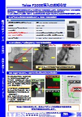
Announcement of the introduction of Talos F200E
Our company will introduce the FEI "Talos F200E" transmission electron microscope system. Compared to conventional models, the resolution for TEM and STEM has improved, and performance has been significantly enhanced, allowing for EDS analysis with four detectors. Additionally, it is equipped with features such as drift-corrected frame integration (DCFI), which accumulates multiple frames while correcting for drift.
-

Power device failure location / Slice & View three-dimensional reconstruction
I will introduce the three-dimensional reconstruction of failure locations using the Slice & View function of FIB-SEM. Continuous SEM images of the structure are obtained, and the resulting images are corrected for positional misalignment between the SEM images and visualized in three dimensions using 3D construction software (Avizo). By combining the position identification technique for cross-sectioning the failure location with the Slice & View function, it is possible to obtain continuous SEM images that retain the defective state and include information before and after the abnormal area.
Recommended products


Distributors

Aites was established in 1993, originating from the quality assurance department of the IBM Japan Yasu office. Based on the technical expertise cultivated through cutting-edge defect analysis and reliability assurance of electronic components at the IBM Japan Yasu office, we have provided various products and services that support the development and manufacturing of semiconductors, displays, organic EL, solar cells, and electronic components to customers both domestically and internationally.