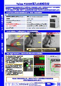
Analysis of electronic components and materials using TEM.

TEM (Transmission Electron Microscope) meets a wide range of requirements for observing failure sites of electronic components, length measurements, elemental analysis, crystal structure analysis, and material evaluation.
TEM can perform not only high-magnification observation but also elemental analysis using EDS and EELS, as well as analysis of crystal structure, surface orientation, lattice constants, and more through electron diffraction.
basic information
■The defective area identified by emission luminescence will be observed while thinning it using FIB. ■Using a TEM with an acceleration voltage of 400kV, which has a high electron transmission capability, we can repeatedly perform transmission observation and FIB processing while confining the defective area within the sample thickness to obtain the optimal image. ■The TEM image magnification can be calibrated in advance, allowing for length measurements with an error of less than 2%.
Price information
We will provide a quote as needed based on the content.
Delivery Time
Applications/Examples of results
- TEM observation of specific areas (application to semiconductor failure sites) - Elemental analysis, electron diffraction (EDS, EELS, electron diffraction images) * Analysis of semiconductor products such as TFT failure analysis and MOS FET failure analysis * Structural analysis of LSI
catalog(12)
Download All Catalogs


News about this product(1)

Recommended products


Distributors

Aites was established in 1993, originating from the quality assurance department of the IBM Japan Yasu office. Based on the technical expertise cultivated through cutting-edge defect analysis and reliability assurance of electronic components at the IBM Japan Yasu office, we have provided various products and services that support the development and manufacturing of semiconductors, displays, organic EL, solar cells, and electronic components to customers both domestically and internationally.