Backside light emission analysis of SiC devices


Pre-processing of SiC devices → Identification of leakage points → Physical analysis/component analysis handled seamlessly!
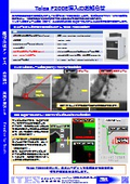
Our company conducts "Backside Emission Analysis of SiC Devices." SiC is a power device with less energy loss compared to conventional Si semiconductors and is attracting attention. However, due to its different physical properties from Si semiconductors, new methods are required for failure analysis. In a case study of backside emission analysis of SiC MOSFETs, an overseas SiC MOSFET was subjected to ESD, creating a G-(D,S) leakage, and numerous emissions indicating the leakage points were detected through emission analysis. When the emission points were observed using TEM, destruction of the SiO2 film and damage to the SiC crystal were noted. *For more details, please refer to the PDF document or feel free to contact us.
basic information
For more details, please refer to the PDF document or feel free to contact us.
Price range
Delivery Time
Applications/Examples of results
For more details, please refer to the PDF document or feel free to contact us.
catalog(6)
Download All Catalogs


News about this product(1)

Recommended products


Distributors

Aites was established in 1993, originating from the quality assurance department of the IBM Japan Yasu office. Based on the technical expertise cultivated through cutting-edge defect analysis and reliability assurance of electronic components at the IBM Japan Yasu office, we have provided various products and services that support the development and manufacturing of semiconductors, displays, organic EL, solar cells, and electronic components to customers both domestically and internationally.