Power semiconductor analysis service


We will handle everything from the evaluation of the diffusion layer to physical analysis/chemical analysis regarding the malfunctioning part!
At Aites Co., Ltd., we offer analysis services for power semiconductors. Since our separation and independence from the Quality Assurance Department of IBM Japan's Yasu office in 1993, we have cultivated our own unique analysis and evaluation techniques. We can handle not only Si semiconductors but also the trending wide bandgap semiconductors. 【Features】 ■ OBIRCH analysis supports not only Si but also SiC and GaN devices ■ FIB processing is possible from either side ■ Visualization of the depletion layer formed at the PN junction ■ Elemental analysis such as EDS and EELS is also supported *For more details, please refer to the PDF document or feel free to contact us.
basic information
[Support from fault location identification to physical analysis such as diffusion layer evaluation and crystal structure] ■ Fault location identification using backside illumination/OBIRCH analysis ■ High-precision positioning and FIB processing at the fault location ■ FIB/LV-SEM observation of defective areas and diffusion layer shape evaluation through EBIC analysis ■ Crystal structure observation and elemental analysis through TEM observation *For more details, please refer to the PDF document or feel free to contact us.*
Price range
Delivery Time
Applications/Examples of results
For more details, please refer to the PDF document or feel free to contact us.
catalog(13)
Download All Catalogs


News about this product(4)
-

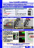
Announcement of the introduction of Talos F200E
Our company will introduce the FEI "Talos F200E" transmission electron microscope system. Compared to conventional models, the resolution for TEM and STEM has improved, and performance has been significantly enhanced, allowing for EDS analysis with four detectors. Additionally, it is equipped with features such as drift-corrected frame integration (DCFI), which accumulates multiple frames while correcting for drift.
-

Strain measurement of power module package resin.
We would like to present the results of strain measurements conducted by attaching strain gauges and thermometers to the surfaces of power modules, both in the mounted state on a circuit board and in the unmounted state. In the mounted module, a slight delay in temperature change was observed, and correspondingly, the change in strain also appeared to be delayed. This is believed to be due to the slower transfer of heat to the module when it is mounted. At Aites, we conduct temperature cycle tests and temperature-humidity cycle tests, during which we can simultaneously measure the strain occurring in the mounted components. Please feel free to consult with us.
-

Power device failure location / Slice & View three-dimensional reconstruction
I will introduce the three-dimensional reconstruction of failure locations using the Slice & View function of FIB-SEM. Continuous SEM images of the structure are obtained, and the resulting images are corrected for positional misalignment between the SEM images and visualized in three dimensions using 3D construction software (Avizo). By combining the position identification technique for cross-sectioning the failure location with the Slice & View function, it is possible to obtain continuous SEM images that retain the defective state and include information before and after the abnormal area.
-

IOL testing of discrete semiconductors
Our company conducts "IOL testing of discrete semiconductors." We repeatedly turn the power ON/OFF in a room temperature environment, applying stress to the device due to temperature changes caused by the device's own heat generation during power ON. During power OFF (cooling), forced cooling is also performed using a fan. Additionally, before conducting the tests, we use representative samples to make adjustments to reach the test temperature conditions. It is possible to adjust the current/time during heating and the fan capacity/timing during cooling.
Recommended products


Distributors

Aites was established in 1993, originating from the quality assurance department of the IBM Japan Yasu office. Based on the technical expertise cultivated through cutting-edge defect analysis and reliability assurance of electronic components at the IBM Japan Yasu office, we have provided various products and services that support the development and manufacturing of semiconductors, displays, organic EL, solar cells, and electronic components to customers both domestically and internationally.