Announcement of the Introduction of FIB-SEM Helios 5 UC

Cross-section production of soft materials has also been realized! 3D reconstruction is possible with Auto Slice & View!
The introduction of the "FIB-SEM Helios 5 UC" is scheduled to start service in November! We will provide shorter delivery times and reliable feedback than ever before. We will achieve high-throughput cross-sectional observation and analysis of a wide range of materials, from semiconductor devices such as power devices, ICs, solar cells, and light-emitting elements, to electronic components like MLCCs and soft materials. With a high-quality beam of up to 100nA, we can process large areas quickly, and by finishing the FIB at low acceleration, it is possible to produce high-quality samples with minimal damage layers. 【Main Features of Helios 5 UC】 ■ High-speed, large-area FIB processing ■ Reduced damage layers through low-acceleration finishing ■ Cryo-FIB processing ■ 3D imaging ■ Complete automation of TEM sample preparation *For more details, please refer to the PDF document or feel free to contact us.
basic information
【Overview of FIB-SEM Composite Device】 ■ SEM column mounted vertically and FIB column mounted diagonally ■ Real-time observation of FIB processing using SEM ■ Improved processing position accuracy ■ Observation and analysis possible without exposure to the atmosphere *For more details, please refer to the PDF document or feel free to contact us.
Price range
Delivery Time
Applications/Examples of results
For more details, please refer to the PDF document or feel free to contact us.
catalog(11)
Download All Catalogs


News about this product(3)
-

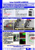
Announcement of the introduction of Talos F200E
Our company will introduce the FEI "Talos F200E" transmission electron microscope system. Compared to conventional models, the resolution for TEM and STEM has improved, and performance has been significantly enhanced, allowing for EDS analysis with four detectors. Additionally, it is equipped with features such as drift-corrected frame integration (DCFI), which accumulates multiple frames while correcting for drift.
-

Power device failure location / Slice & View three-dimensional reconstruction
I will introduce the three-dimensional reconstruction of failure locations using the Slice & View function of FIB-SEM. Continuous SEM images of the structure are obtained, and the resulting images are corrected for positional misalignment between the SEM images and visualized in three dimensions using 3D construction software (Avizo). By combining the position identification technique for cross-sectioning the failure location with the Slice & View function, it is possible to obtain continuous SEM images that retain the defective state and include information before and after the abnormal area.
-

Announcement of the Introduction of FIB-SEM Helios 5 UC
The introduction of the "FIB-SEM Helios 5 UC" is scheduled to start service in November. We will provide shorter delivery times and reliable feedback than before. We will achieve high-throughput cross-sectional observation and analysis of a wide range of materials, from semiconductor devices such as power devices, ICs, solar cells, and light-emitting elements to electronic components like MLCCs and soft materials. With a high-quality beam of up to 100nA, we can process large areas at high speed, and by finishing the FIB at low acceleration, it is possible to produce high-quality samples with minimal damage layers. You can view related products and catalogs.
Recommended products


Distributors

Aites was established in 1993, originating from the quality assurance department of the IBM Japan Yasu office. Based on the technical expertise cultivated through cutting-edge defect analysis and reliability assurance of electronic components at the IBM Japan Yasu office, we have provided various products and services that support the development and manufacturing of semiconductors, displays, organic EL, solar cells, and electronic components to customers both domestically and internationally.