
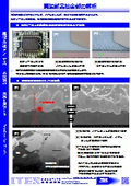
Comparison of cross-sectional observation images

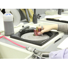




We will introduce suitable observation methods for cross-sectional observation of chip resistors and copper wiring sections!
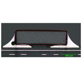
To assist you in selecting an observation device, we will introduce the differences in visibility between a metal microscope, W-SEM, and FE-SEM. When observing the cross-section of a chip resistor, certain areas may be difficult to observe at low magnification with a metal microscope, but with SEM observation, the greater depth of field allows for high-flatness images even at low magnification. When observing the cross-section of copper wiring, the copper-resin interface and the condition inside cracks can be observed with W-SEM, but with FE-SEM, even the crystal grains and tiny voids at the connection interface can be clearly observed. [Comparison] ■ Cross-section observation of chip resistors: Comparison of images between metal microscope and W-SEM ■ Cross-section observation of copper wiring: Comparison of images between W-SEM and FE-SEM *For more details, please download the PDF or feel free to contact us.
basic information
For more details, please download the PDF or feel free to contact us.
Price range
Delivery Time
Applications/Examples of results
For more details, please download the PDF or feel free to contact us.
catalog(7)
Download All Catalogs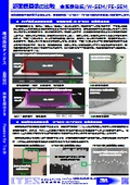

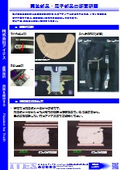
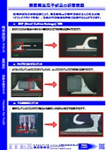


Recommended products


Distributors

Aites was established in 1993, originating from the quality assurance department of the IBM Japan Yasu office. Based on the technical expertise cultivated through cutting-edge defect analysis and reliability assurance of electronic components at the IBM Japan Yasu office, we have provided various products and services that support the development and manufacturing of semiconductors, displays, organic EL, solar cells, and electronic components to customers both domestically and internationally.