

Product Categories
-

◉ nanoETCH Soft Etching Device
-

MiniLab Series Experimental Equipment
-

◉ 【MiniLab-026】Small Vacuum Deposition Device
-
![A semi-custom-made thin film experimental device that can be flexibly assembled according to your desired configuration, including deposition, sputtering, EB, and annealing modules.
Possible combinations from the following deposition sources:
- Resistance heating deposition source x up to 4
- Organic deposition source x up to 4
- Electron beam deposition
- 2-inch magnetron sputtering cathodes x 4
[Main Specifications]
- SUS304 60ℓ volume chamber 400x400x400mm
- Pump: Turbo molecular pump, rotary pump (dry pump also available)
- Vacuum exhaust: Automatic control of vacuum/vent
- Metal film deposition: Up to 4 points
- Organic film deposition: Up to 4 points
- EB electron beam deposition source: 7cc crucible x 6 (or 4cc crucible x 8)
- Φ2 to 4 inch magnetron sputtering cathodes x up to 4
- Process control: Manual/automatic multilayer film and simultaneous deposition, APC automatic control available (*optional)
- Film thickness monitor: Quartz crystal oscillator sensor head x 2
- Utilities: Power supply 200V three-phase 13A, water cooling 3ℓ/min, N2 vent gas 0.1Mkpa
- Other options: Substrate heating, cooling, substrate elevation/rotation, bias stage, dry pump, load lock](https://image.mono.ipros.com/public/premium/image_category/b1f/408104/IPROS63777749693352850763.jpeg?w=140&h=140)
◉ 【MiniLab-060】Flexible Thin Film Experimental Device
-

◉ 【MiniLab-080】Flexible Thin Film Experimental Device
-

◉ 【MiniLab-090】Flexible Thin Film Experimental Device
-

MiniLab-026/090 Glove Box Thin Film Experiment Device
-

□■□Thin Film Experiment Device (Compact Type)□■□
-

◉ nanoPVD-S10A Magnetron Sputtering Device
-

◆nanoPVD-T15A◆ High-performance organic and metal film deposition device
-

◆ANNEAL◆ Wafer Annealing Equipment
-

◉ nanoCVD-8G/8N Graphene/CNT Synthesis Device
-
![Multi-purpose, high-precision process control [Hot-wall thermal CVD system]
◉ Maximum operating temperature 1100℃
◉ Graphene, carbon nanotubes
◉ ZnO nanowires
◉ Insulating films such as SiO2
Additionally, it can be utilized for a wide range of applications as a hot-wall thermal CVD system.](https://image.mono.ipros.com/public/premium/image_category/b1f/408104/IPROS06047929671708728741.jpeg?w=140&h=140)
◉ Nanofurnace "BWS-NANO" Thermal CVD Device
-

◇◆Film-Forming Component◆◇
-

Ultra-High Temperature Small Experimental Furnace Series
-

◉ Mini-BENCH Ultra High Temperature Small Tabletop Experimental Furnace Max 2200℃
-

◉ TCF-C500 Ultra High Temperature Small Experimental Furnace Max 2900℃
-

● MiniLab-WCF Ultra-High Temperature Wafer Annealing Furnace 2200℃
-

◆◇◆ Small Vertical Experimental Furnace for R&D TVF-110 ◆◇◆
-

□■□ Substrate Heating Heater □■□
-

◉ BH Series substrate heating heater Max 1600℃
-

◉ SH series substrate heating heater Max 1100℃
-

◉ Hot stage "Substrate heating mechanism" Max 1800℃
-

◆HTE Heater◆ High Vacuum Crucible Heating Heater Max 1500℃
-

Temperature Sensor
-

Infrared thermometer measuring device
-

◉ Small, high-precision infrared radiation temperature sensor
-

◉ USB connection type, variable emissivity high-temperature infrared radiation temperature sensor
-

◉ Intrinsically Safe Explosion-Proof Infrared Radiation Temperature Sensor
-

◉ Smartphone-configured infrared radiation temperature sensor
Featured products


Products/Services(56items)

![Wafer Scale Graphene Synthesis Device [nanoCVD-WGP]](https://image.mono.ipros.com/public/product/image/f9c/2000984153/IPROS42037887099773798497.jpeg?w=280&h=280)
![Sputtering/Dual Chamber System [MiniLab]](https://image.mono.ipros.com/public/product/image/17e/2000781209/IPROS98663158405637428301.jpeg?w=280&h=280)
news list
-
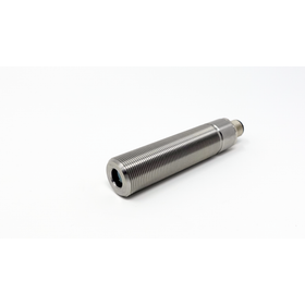
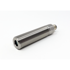
【PyroCV】Infrared Temperature Sensor for Construction Machinery and Work Vehicles
PyroCV is suitable for temperature measurement of asphalt and non-reflective building materials. It can also be widely used for temperature measurement of non-ferrous metals, concrete, and painted surfaces that do not reflect. ● Stable high-speed response performance: 125 msec ● Two types of output options: voltage output (0-5V), CAN BUS communication output ● Durability: Robust body made of SUS316, protection rating IP67/IP65 ● Compliance standard: Conforms to EMC standards ISO 13766-1 for construction machinery ● Rugged design that can withstand the harsh environments of road paving work ● Equipped with M12 (5-pin) waterproof connector for easy wiring and disconnection PyroCV is suitable for tests that comply with the electrical load testing standard ISO 16750-2 for automotive equipment. Additionally, compliance with ISO 13766-1 provides load dump surge suppression while maintaining equivalent performance to the same electrical system. 【Main Applications】 ⚪︎ Asphalt paving ⚪︎ Road rollers ⚪︎ Concrete processing and curing, etc.
-
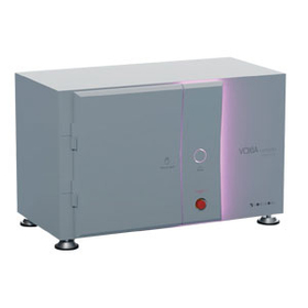
VOXIA compact X-ray CT imaging device
Compact design with a space-saving layout that can be installed anywhere. Despite its compact body, it generates high-resolution data through advanced calculation software. * X-ray tube voltage: 20-90kV, or 40-maximum 130kV * Focus diameter: 7μm (5μm@4W) * Detector pixel: 89μm, approximately 3.2 million pixels! * Sample size: Φ120mm ◉ Vcap (Control Software): A custom-made imaging stage tailored to the subject and purpose. A series of tasks from shooting to image output can be performed with just a click. High-speed continuous shooting in as fast as 20 seconds, with processing from shooting start to image reconstruction taking about 30 seconds. ◉ VCT (Reconstruction Software): Customizable automatic measurement and analysis software specialized for the specified subject. High-speed reconstruction of shooting data with 992 x 992 pixel images and 600 projections in just 3.8 seconds! ◉ MolcerPlus (3D Display Analysis): Custom software that enables measurement conditions that were difficult with conventional software. Software for displaying, processing, and measuring the imaged object. ● High safety, ● Compatible with a wide variety of samples, ● Intuitive HMI, easy operation.
-
VOXIA box X-ray CT imaging device
Compact design with a space-saving layout that can be installed anywhere. Despite its compact body, it generates high-resolution data through advanced calculation software. * X-ray tube voltage: 0–150kV * Focus diameter: 7μm (5μm@4W) * Detector pixel: 49.5μm, 6.75 million pixels! * Sample size: Φ100mm ◉ Vcap (control software): A custom-made imaging stage tailored to the subject and purpose. A series of tasks from shooting to image output can be performed with just a click. High-speed continuous shooting in as fast as 20 seconds, with processing from shooting start to image reconstruction taking about 30 seconds. ◉ VCT (reconstruction software): Customizable automatic measurement and analysis software specialized for the specified subject. High-speed reconstruction of shooting data with an image size of 992 x 992 pixels and 600 projections in just 3.8 seconds! ◉ MolcerPlus (3D display analysis): Custom software that enables measurement conditions that were difficult with conventional software. Software for displaying, processing, and measuring the imaged object. ● High safety, ● Compatible with a wide variety of samples, ● Intuitive HMI, easy operation.
-
Vacuum deposition device □■□【MiniLab-LT080A】□■□ Capable of various deposition applications such as resistance heating, organic deposition, and electron beam deposition.
The ML-080, with a volume of 80 liters and dimensions of 400(W)x400(D)x570(H)mm, is composed of a D-type box chamber. It has the same configuration as the 070 model but features a taller chamber, resulting in a longer TS distance adjustment range and improved film uniformity during deposition on large-diameter substrates, making it an optimal model for vacuum deposition. It is a higher-end model than the ML-070, which can also accommodate a load lock mechanism. Like the 070, it is compact yet supports a wide range of applications including resistance heating deposition (for metals, insulators, and organic materials), electron beam deposition, RF/DC/PulseDC compatible magnetron sputtering, RIE plasma etching, and annealing. - Maximum substrate size: Φ11 inch - Resistance heating deposition source x up to 4 units - Organic deposition source x up to 4 units - Magnetron sputtering cathode x 4 units - Electron beam deposition - Substrate heating stage (standard 500℃, Max 1000℃) - *Plasma etching / <30W soft etching *Plasma etching can be installed in both the main chamber and the load lock chamber.
-
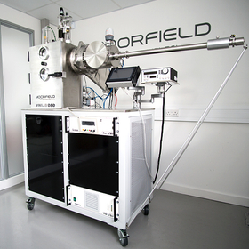
□■□【MiniLab-080】Flexible Thin Film Experimental Device□■□ Can be configured flexibly according to requirements for processes such as deposition, sputtering, EB deposition, and organic deposition.
The ML-080, with a volume of 80 liters and dimensions of 400(W)x400(D)x570(H)mm, is composed of a D-type box chamber. It has the same configuration as the 070 model but features a taller chamber, which extends the TS distance adjustment range and improves film uniformity during deposition on large-diameter substrates, making it an optimal model for vacuum deposition. It is a higher-end model than the ML-070, which can also add a load lock mechanism. Like the 070, it is compact yet supports a wide range of applications including resistance heating deposition (for metals, insulators, and organic materials), EB deposition, RF/DC/PulseDC compatible magnetron sputtering, RIE plasma etching, and annealing. - Maximum substrate size: Φ11 inch - Resistance heating deposition sources x up to 4 units - Organic deposition sources x up to 4 units - Magnetron sputtering cathodes x 4 units - Electron beam deposition - Substrate heating stage (standard 500℃, Max 1000℃) - *Plasma etching / <30W soft etching *Plasma etching can be installed in both the main chamber and the load lock chamber.

Aboutテルモセラ・ジャパン
本社
Professional Thermal Engineering. We will contribute to Japan's research and development in thermal application technology.
【Endless possibility_thermal engineering...】 Our company sells vacuum thin film devices for semiconductor and electronic device fundamental research, ultra-high temperature heaters for CVD substrate heating, experimental furnaces, temperature measurement equipment, and more. To meet the endless demand for "heat," which is indispensable in any era, and to respond to various requests in the field of fundamental technology development, we aim to introduce the latest equipment and contribute to research and development in Japan.