
Compound Composite Testing Device


Effective for wafer inspection up to 6 inches! A compound wafer inspection device capable of inspection in the same coordinate system.
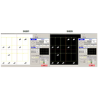
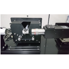
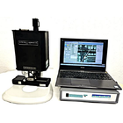
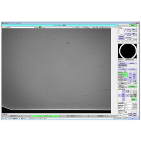
This product is a compound wafer inspection device effective for inspecting internal micro-pipes, delamination, surface scratches, foreign substances, and polishing marks on SiC, GaN, and sapphire wafers up to 6 inches. It features four optical systems for inspection: super macro, differential interference, dark field, and transmission, all equipped with autofocus, allowing inspections to be conducted in the same coordinate system via an automatic stage. Optionally, AFM and wafer thickness measurement can also be added in the same coordinate system. 【Features】 - Equipped with four optical systems (super macro, differential interference, dark field, transmission) - All optical systems have autofocus functionality - Inspections can be performed in the same coordinate system using an automatic stage - Option to add AFM and wafer thickness measurement *For more details, please download the PDF or feel free to contact us.
basic information
【Specifications】 ■ Super Macro (SM-75): Observation of local wafer Schlieren images and synthesis processing of local images to create a full wafer image. ■ Differential Interference Microscopy Image Station: Observation of local wafer dark field and bright field microscopy images. ■ Dark Field Oblique Light Image Station: Observation of dark field oblique light images of the local wafer surface. ■ Polarized Transmission Image Station: Observation of polarized transmission images of the local wafer surface. ■ Automatic Stage: Each station is integrated into a single structure, enabling work movement and coordinate linkage between units. *For more details, please download the PDF or feel free to contact us.
Price range
Delivery Time
Applications/Examples of results
【Applications (Partial)】 ■ Inspection of micro-pipes and voids inside the wafer ■ Surface scratch inspection, polishing mark inspection ■ Foreign matter inspection (including internal) ■ Measurement of surface roughness and pattern inclination, etc. (optional AFM) ■ Inspection of scratches, pits, and bubbles ■ Non-contact thickness measurement (optional thickness gauge) *For more details, please download the PDF or feel free to contact us.
catalog(1)
Download All Catalogs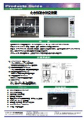
Recommended products
Distributors

Since our company's establishment in 1986, we have long been engaged in semiconductor-related businesses that support Japan's cutting-edge technology. On the hardware side, we have developed construction and manufacturing environments, including clean rooms. On the human resources side, we have focused on training semiconductor engineers and establishing a service system that can promptly respond to customer needs. Last year, we participated in SEMICON Japan for the first time, and by directly interacting with many industry stakeholders, we were able to learn again what is currently needed and what services should be created. At the same time, the morale within the company has been rising, and we are actively conducting sales activities. It is said that the Japanese economy is finally showing signs of recovery. However, even just looking at the semiconductor industry, the entry of overseas manufacturers and the significant improvement in technology and services are remarkable, so we aim to enhance our international competitiveness in our sales expansion. Not only domestically but also in response to the era of globalization, our role as a hub connecting North America and Asia, especially given our excellent airport access, will further increase.