
Backside crack inspection device


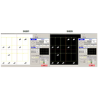
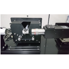
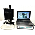
The measurement accuracy is constant and does not depend on the skill of the operator. It achieves stable inspection quality during continuous operation.
The "Back Surface Crack Inspection Device" is an automatic inspection device for ceramic substrates that can be easily constructed for 24-hour inline automation. It detects fine cracks that are difficult to see with the naked eye using image processing with special lighting from two directions. The non-contact inspection measurement prevents damage to the workpiece, and the fast measurement speed is an advantage. Results are automatically saved as data, and automatic judgment of good and defective products is performed, with support for alert output in case of defects. Products inspected can be guaranteed for quality. The device can be constructed with any desired takt time and inspection accuracy. 【Features】 ■ Detection of fine cracks using special lighting from two directions and image processing ■ Non-contact inspection measurement that does not damage the workpiece ■ Automatic data saving and automatic judgment of results (good/defective) ■ Automatic alert output in case of defects ■ Construction possible with any desired takt time and inspection accuracy *For more details, please download the PDF or feel free to contact us.
basic information
【Specifications】 ■Camera: 25 million pixel CMOS camera ■Lens: High-precision lens for FA ■Lighting method: Bidirectional line lighting and coaxial lighting ■Lighting power supply: USB control via PC ■Field of view size: Approximately 58mm x 58mm ■Tact time: 1 second or less per field of view *For more details, please download the PDF or feel free to contact us.
Price range
Delivery Time
Applications/Examples of results
【Purpose】 ■Automatic inspection of cracks on the back surface of ceramic substrates *For more details, please download the PDF or feel free to contact us.
catalog(1)
Download All Catalogs
Recommended products
Distributors

Since our company's establishment in 1986, we have long been engaged in semiconductor-related businesses that support Japan's cutting-edge technology. On the hardware side, we have developed construction and manufacturing environments, including clean rooms. On the human resources side, we have focused on training semiconductor engineers and establishing a service system that can promptly respond to customer needs. Last year, we participated in SEMICON Japan for the first time, and by directly interacting with many industry stakeholders, we were able to learn again what is currently needed and what services should be created. At the same time, the morale within the company has been rising, and we are actively conducting sales activities. It is said that the Japanese economy is finally showing signs of recovery. However, even just looking at the semiconductor industry, the entry of overseas manufacturers and the significant improvement in technology and services are remarkable, so we aim to enhance our international competitiveness in our sales expansion. Not only domestically but also in response to the era of globalization, our role as a hub connecting North America and Asia, especially given our excellent airport access, will further increase.