[TEM ED-Map] TEM Electron Diffraction Mapping Method

This is a method for analyzing the orientation distribution of crystalline samples using electron diffraction in a transmission electron microscope (TEM).
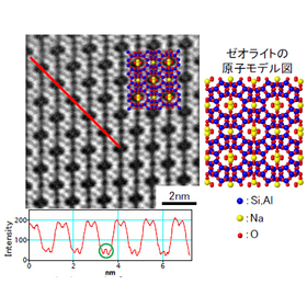
By scanning the electron beam probe and measuring the electron diffraction patterns at each point, high spatial resolution crystal information can be obtained. This method allows for the acquisition of information on smaller crystal grains than the EBSD method in SEM. It is also referred to as ACOM (Automated Crystal Orientation Mapping) - TEM method. - Crystal grain size analysis is possible - Orientation measurement of the measurement area is possible - Observation of twin grain boundaries (corresponding grain boundaries) is possible - Extraction of specific crystal orientations is possible - Measurement of the rotation angle of adjacent crystal grains is possible - Evaluation of crystal grains larger than a few nanometers is possible
basic information
For more details, please contact us.
Price range
Delivery Time
Applications/Examples of results
- Evaluation of grain size in polycrystalline thin films - Evaluation of grain size of crystals present in amorphous materials - Evaluation of crystal orientation
Recommended products


Distributors

MST is a foundation that provides contract analysis services. We possess various analytical instruments such as TEM, SIMS, and XRD to meet your analysis needs. Our knowledgeable sales representatives will propose appropriate analysis plans. We are also available for consultations at your company, of course. We have obtained ISO 9001 and ISO 27001 certifications. Please feel free to consult us for product development, identifying causes of defects, and patent investigations! MST will guide you to solutions for your "troubles"!