[Measurement Method] Electron Microscopy Observation and Analysis
![[Measurement Method] Electron Microscopy Observation and Analysis](https://image.mono.ipros.com/public/premium/image_category/099/387108/IPROS3455379713280402900.jpg?w=140&h=140)
[Measurement Method] Electron Microscopy Observation and Analysis
◆AES (Auger Electron Spectroscopy) ◆SEM (Scanning Electron Microscopy) ◆EBIC (Electron Beam Induced Current) ◆EBSD (Electron Backscatter Diffraction) ◆EDX (Energy Dispersive X-ray Spectroscopy) ◆EPMA (Electron Probe Microanalysis) ◆TEM (Transmission Electron Microscopy) ◆EELS (Electron Energy Loss Spectroscopy) ◆SIM (Scanning Ion Microscopy)
1~28 item / All 28 items
-

[AES] Auger Electron Spectroscopy
By measuring the kinetic energy distribution of Auger electrons emitted by electron beam irradiation, insights can be gained regarding the types and quantities of elements present on the sample surface.
last updated
-

Scanning Electron Microscopy (SEM)
High magnification observation (up to about 300,000 times) is possible.
last updated
-

[EBIC] Electron Beam Induced Current
A method to obtain information about the electric field structure inside the sample (junction structure of semiconductors).
last updated
-

[EBSD] Electron Backscatter Diffraction Method
It is possible to easily obtain crystal information over a wide area.
last updated
-

[SEM-EDX] Energy Dispersive X-ray Spectroscopy (SEM)
It is a method for conducting elemental analysis and compositional analysis by detecting characteristic X-rays generated by electron beam irradiation and spectrally analyzing them by energy.
last updated
-

[Slice&View] Three-Dimensional SEM Observation Method
By repeatedly performing cross-sectioning processing with FIB and observation with SEM, and reconstructing the obtained images, three-dimensional structural information can be obtained.
last updated
-

(S)TEM (Scanning Transmission Electron Microscopy)
Elemental analysis, state evaluation, particle size analysis, and acquisition of three-dimensional structural images at the nanoscale.
last updated
-

[TEM-EELS] Electron Energy Loss Spectroscopy
By measuring the energy lost due to interactions with atoms as electrons pass through thin film samples, the constituent elements and electronic structure of the material can be analyzed.
last updated
-

[ED] Electron Diffraction Method
ED is a method for investigating crystal structures from diffraction patterns obtained by irradiating a sample with an electron beam.
last updated
-

[SIM] Scanning Ion Microscopy Method
Observation of SIM images is possible with high resolution (accelerating voltage 30kV: 4nm).
last updated
-

[TEM-EDX] Energy Dispersive X-ray Spectroscopy (TEM)
EDX is a method that measures the energy and occurrence of characteristic X-rays generated when an electron beam is irradiated onto the analysis area, allowing for elemental analysis and compositional analysis.
last updated
-

[Analysis Case] Degradation Analysis of Liquid Crystal Displays
We will comprehensively evaluate liquid crystals, alignment films, sealing materials, TFTs, and more.
last updated
-

[Analysis Case] Cell Cycle Assessment from Bacterial Images
By using deep learning and data analysis, we can evaluate sample characteristics by utilizing large amounts of data.
last updated
-

[TEM ED-Map] TEM Electron Diffraction Mapping Method
This is a method for analyzing the orientation distribution of crystalline samples using electron diffraction in a transmission electron microscope (TEM).
last updated
-

[Analysis Case] Evaluation of Two-Dimensional Electron Gas Layer in Normally Off GaN HEMT
We can offer a one-stop solution for comprehensive analysis of product research.
last updated
-

[Analysis Case] Trench-type Si-MOSFET IDSS Leakage Location Analysis
One-stop service from identifying device defects to analyzing causes.
last updated
-

[Analysis Case] Failure Analysis of SiC Transistor using Slice & View
Check the leak path by 3D visualization of SEM images.
last updated
-

[Analysis Case] Component Analysis of Leakage Areas in SiC Power Transistors
It is possible to perform magnified observation and EDX analysis at the gate destruction location identified by Slice & View.
last updated
-

[EPMA] Electron Probe Micro Analyzer
By analyzing the characteristic X-rays generated when a finely focused electron beam is irradiated onto the surface of a solid sample in a vacuum, insights can be gained regarding the identification of elements and quantitative values.
last updated
-

Identification of resistance anomalies due to absorption current
You can identify high resistance and open areas in the wiring from the absorption current image.
last updated
-

Structural analysis using Xe-plasma FIB.
Precision processing/structural evaluation is possible over a wide area of several hundred micrometers.
last updated
-

[Analysis Case] Lithium-ion Secondary Battery
Accurate evaluation of the separator cross-sectional shape through sample cooling.
last updated
-

[Analysis Case] STEM, EBSD Image Simulation for Polycrystalline Structure Analysis
Evaluation of crystal forms using simulations.
last updated
-

[Analysis Case] Analysis of All-Solid-State Batteries
Comprehensive analytical evaluation combining structure, composition, and electrical properties.
last updated
-

[Analysis Case] Structural Evaluation of Secondary Battery Separators
Evaluation of the shape and composition of organic/inorganic multilayer structures.
last updated
-

[Analysis Case] Evaluation of Resistance Values and Li Distribution in Secondary Battery Cathodes
Distribution of resistance values in the electrode cross-section, visualization of conduction paths, and comparison with ion distribution.
last updated
-

[Analysis Case] Comprehensive Evaluation of Positive Electrode Active Materials in Secondary Batteries
Proposing an evaluation that combines structure, composition, and electricity to solve development issues.
last updated
-
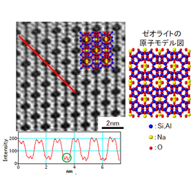
[Analysis Case] Evaluation of Solution Components Before and After Adsorption and Zeolite Structure
We capture the ion exchange process from the ion content in the solution and the structural changes of the adsorbent.
last updated