[SIM] Scanning Ion Microscopy Method


Observation of SIM images is possible with high resolution (accelerating voltage 30kV: 4nm).
- SIM imaging observation is possible with high resolution (accelerating voltage 30kV: 4nm). - Compared to SEM images, SIM images provide information about the extreme surface layer. - Observation of metal crystal grains is possible (e.g., Al, Cu). - The resolution is inferior to SEM images (SIM: 4nm, SEM: 0.5nm). ■Features of MST-owned equipment - Compatible with JEIDA standard wafers with a maximum sample size of 300mm in diameter. - Continuous cross-sectional SIM imaging acquisition is possible in combination with FIB (Focused Ion Beam) processing (Slice & View).
basic information
When an ion beam is irradiated onto a solid sample, secondary electrons are generated. These secondary electrons produce contrast according to the crystal orientation of each grain. This image is referred to as a Scanning Ion Microscope (SIM) image. Although similar contrast images can also be obtained by electron beam irradiation, the contrast is more pronounced with ion beams. By observing the SIM images of polycrystalline metals, it is possible to gain insights into the size and distribution of the crystal grains.
Price range
Delivery Time
Applications/Examples of results
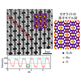
- Visualization of current paths through cross-sectional observation (conductive contrast) - Observation of crystal grains such as Al, Cu, and Fe (channeling images) - Crystal grain size analysis using multi-angle inclination
Detailed information
-

Please consult with us first. ★ We will start with a proposal for an analysis plan ★ We can, of course, meet at your company for discussions. We will carefully explain the analysis results and leave no questions unanswered. Please contact us at 03-3749-2525 or info@mst.or.jp!
-

We will hold a visiting seminar. ★ We offer free seminars with engineers tailored to our customers' needs ★ We will introduce analytical techniques and explain analytical data according to your requests. ◆ Examples of seminar content - A broad explanation of MST's analytical methods - A detailed explanation of specific analytical methods from the principles - An explanation of the analytical data requested by the customer Please contact us at 03-3749-2525 or info@mst.or.jp!
catalog(1)
Download All Catalogs
Recommended products


Distributors

MST is a foundation that provides contract analysis services. We possess various analytical instruments such as TEM, SIMS, and XRD to meet your analysis needs. Our knowledgeable sales representatives will propose appropriate analysis plans. We are also available for consultations at your company, of course. We have obtained ISO 9001 and ISO 27001 certifications. Please feel free to consult us for product development, identifying causes of defects, and patent investigations! MST will guide you to solutions for your "troubles"!