[Analysis Case] Binding State Mapping by XPS


It is possible to evaluate the distribution of surface contamination and surface treatment on samples with mm-order precision.
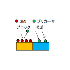
This document presents an example of evaluating organic contamination through bonding state mapping using XPS. This bonding state mapping is obtained by acquiring XPS spectra of the element of interest at several hundred points within the plane and plotting the distribution of peak intensities corresponding to the energy positions of specific bonding states. Depending on the size of the area of interest, evaluation areas can be set to arbitrary sizes ranging from approximately 1mm to 20mm square, making it particularly suitable for assessing contamination, discoloration, and surface treatments on the order of millimeters. Similar evaluations can also be conducted for metals and silicon, in addition to carbon.
basic information
Measurement Method: XPS Product Field: Electronic Components, Manufacturing Equipment, Parts, Daily Goods Analysis Purpose: Bonding State Evaluation
Price range
Delivery Time
Applications/Examples of results
Analysis of electronic components, manufacturing equipment, parts, and daily necessities.
catalog(1)
Download All Catalogs
Recommended products


Distributors

MST is a foundation that provides contract analysis services. We possess various analytical instruments such as TEM, SIMS, and XRD to meet your analysis needs. Our knowledgeable sales representatives will propose appropriate analysis plans. We are also available for consultations at your company, of course. We have obtained ISO 9001 and ISO 27001 certifications. Please feel free to consult us for product development, identifying causes of defects, and patent investigations! MST will guide you to solutions for your "troubles"!