
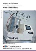
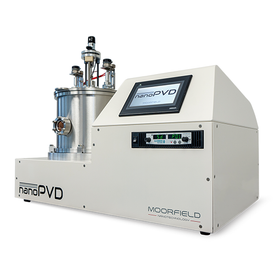
Sputtering and deposition source composite thin film deposition device [nanoPVD-ST15A]


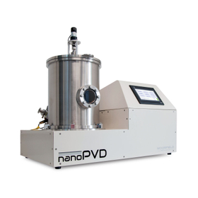


Sputter Cathode and Co-evaporation Source Mixed Thin Film Experimental Device: Metal deposition, organic deposition, and sputter cathode installed in a compact frame.
Three types of film formation components are installed in the chamber: resistance heating evaporation source (metal evaporation), organic evaporation source (organic materials), and magnetron sputtering (metal and insulating materials), allowing for various thin film experimental setups to be accommodated within a single chamber. ◉ Three combinations are available: 1. Sputter cathode + resistance heating evaporation source x2 2. Sputter cathode + organic evaporation source x2 3. Sputter cathode + resistance heating source x1 + organic evaporation source x1 (*DC sputtering only) - Evaporation range: Φ4 inch / Φ100 mm - Vacuum exhaust system: Turbo molecular pump + auxiliary pump (rotary or dry scroll pump) - Substrate rotation and vertical lifting stage - Max 500℃ substrate heating heater - Quartz oscillator film thickness sensor - 7” touch panel HMI operation (includes 'IntelliLink' Windows PC remote monitoring software)
basic information
【Specifications】 ◉ Compatible substrate: up to Φ4 inch ◉ Sputtering: 2" cathode x up to 3 sources ◉ Vacuum deposition: resistance heating deposition (up to 2), organic material deposition (up to 4) ◉ 7" touch panel for easy operation with PLC automatic process control ◉ APC automatic pressure control ◉ High precision process control with MFC ◉ 1 line of Ar gas (standard) + up to 3 additional lines for N2, O2 ◉ USB port for connection to Windows PC, allowing creation and storage of recipes for up to 1000 layers and 50 films. Data logging on PC ◉ Various other options available ◉ 7" touch panel for easy operation with PLC automatic process control
Price information
For more details, please contact our company.
Delivery Time
Model number/Brand name
nanoPVD-ST15A
Applications/Examples of results
Various electronic device thin film experiments Compatible with metal films, insulating films, compound films, and many other applications.
catalog(37)
Download All Catalogs












News about this product(10)
-
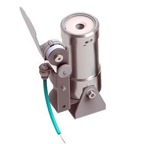
◆OLED◆ Organic vapor deposition - High-temperature metal evaporation source Max 1500℃
The OLED evaporation source is a high-temperature heating heater for vacuum devices with a maximum operating temperature of 1500°C. It can evaporate materials with high evaporation temperatures, making it suitable for a wide range of applications as a vacuum high-temperature heater and evaporation cell, from low-temperature organic deposition (up to 800°C) cells to high-temperature resistance heating deposition (up to 1500°C) MBE cells. Shutter actuators and water-cooled jackets are also available. High-temperature heaters above 800°C are designed with internal shielding, considering insulation and thermal shielding. 【Main Specifications】 ■ Maximum control temperature: 800°C or 1500°C ■ Operating environment: in vacuum or inert gas (*O2 up to 800°C) ■ Heater: tungsten filament ■ Crucible volume: 1cc (maximum fill volume 1.5cc) ■ Crucible material: alumina ■ Case material: SUS304 or molybdenum ■ Thermocouple: K or C 【Options】 ⚫ Crucible material: PBN, graphite, quartz ⚫ Heater: NiCr wire, Kanthal wire (*for O2) ⚫ Crucible volume: 10cc (maximum fill volume 15cc) ⚫ Shutter: pneumatic or motor-driven ⚫ Water-cooled jacket ⚫ Controller (for heater and shutter control)
-

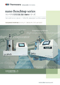
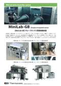
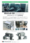
【MiniLab】 Evaporation/Sputtering Dual Chamber System
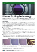
Two thin film experimental devices are connected by a load lock mechanism. Different film deposition devices (sputtering - evaporation, etc.) are seamlessly connected via the load lock. With Moorfield's unique load lock system, connections to the process chamber on the left, right, and rear are also possible (see photo below). 1. MiniLab-E080A (Evaporation Device) - EB evaporation: 7cc crucible x 6 - Resistance heating evaporation x 2 - Organic evaporation limit x 2 2. MiniLab-S060A (Sputtering Device) - Φ2" Magnetron cathode x 4 for simultaneous sputtering - Compatible with both DC and RF power supplies 3. Load Lock Chamber - Plasma etching stage In the load lock chamber, plasma cleaning of the substrate surface is performed using the "RF/DC substrate bias stage," and the company's unique "soft etching" technology allows for a <30W low-power, damage-free plasma etching stage. This enables delicate etching processes that are prone to damage, such as 2D (removal of resists like PMMA), graphene delamination, and etching of Teflon substrates. (*This can also be installed in the main chamber stage.)
-

☆★☆ Spatter and Vapor Deposition Source Combined Film Formation Device 【nanoPVD-ST15A】 ☆★☆
Sputter Cathode and Co-evaporation Source Mixed Thin Film Experimental Device. Metal deposition, organic deposition, and sputter cathode are installed in a compact frame. A resistance heating evaporation source (for metal deposition), an organic evaporation source (for organic materials), and magnetron sputtering (for metals and insulating materials) are installed in the chamber, allowing for various thin film experimental setups within a single chamber. ◉ Three combinations available: 1. Sputter Cathode + Resistance Heating Evaporation Source x2 2. Sputter Cathode + Organic Evaporation Source x2 3. Sputter Cathode + Resistance Heating Source x1 + Organic Evaporation Source x1 (*DC sputtering only) 【Specifications】 ◉ Compatible substrates: up to Φ4 inches ◉ Sputtering: 2" cathode x up to 3 sources ◉ Vacuum deposition: Resistance heating evaporation (up to 2), organic evaporation (up to 4) ◉ 7" touch panel operation with PLC automatic process control ◉ APC automatic pressure control ◉ 1 line of Ar gas (standard) + expandable with N2, O2 ◉ Connects to a Windows PC via USB for recipe creation and storage. Data logging on PC ◉ Various other options available ◉ Easy operation with a 7" touch panel and PLC automatic process control
-

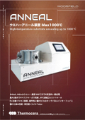
Wafer Annealing Equipment [ANNEAL] Max 1000℃ APC Automatic Pressure Control MFC x3 System Compatible with Φ4 to 6 inch Substrates
Max 1000℃, MFC up to 3 systems, APC pressure control, compatible with substrates from 4" to a maximum of 6", high vacuum annealing device (<5 × 10⁻⁷ mbar) [ANNEAL] is a research and development annealing device capable of high-temperature heat treatment of substrates such as wafers in a stable process atmosphere. It allows high-temperature processing up to 1000℃ using a heating stage installed in a high vacuum water-cooled SUS chamber. A heat shield is installed inside the chamber to ensure safety through interlock. The mass flow controller can be expanded to a maximum of 3 systems, enabling firing operations with precisely adjusted process gas pressure (APC automatic process control system option). Additionally, there are many options available, including a front view port, dry scroll pump, special substrate holder, and additional thermocouples. The heating stage inside the chamber has three variations depending on the process gas atmosphere and treatment temperature: - Halogen lamp heater: Max 500℃ - C/C composite heater: Max 1000℃ (in vacuum, inert gas only) - SiC coating heater: Max 1000℃ (vacuum, inert gas, O2)
-

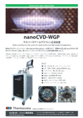
☆★☆★【nanoCVD-WGP】Wafer-scale graphene/carbon nanotube synthesis device ☆★☆★
Plasma CVD equipment compatible with wafer sizes Φ3 inch and Φ4 inch. Rapid synthesis of clean, high-quality graphene while suppressing impurities. Usable with both thermal CVD and low to high temperature plasma CVD methods. The configuration can be customized according to requirements, including mass flow gas supply systems and substrate heating heaters. 【Example of equipment configuration】 - Substrate: Cu, Ni, etc. (film, foil) - Raw materials: CH4, C2H4, solids (PMMA), etc. - Process gases: H2, Ar, N2, etc. - Substrate size: Φ4 inch - 150W, 13.56MHz RF power supply - Substrate heating from 500℃ to Max 1100℃ - High precision process gas pressure APC control - Mass flow controller with a maximum of 4 channels
Recommended products




Distributors

【Endless possibility_thermal engineering...】 Our company sells vacuum thin film devices for semiconductor and electronic device fundamental research, ultra-high temperature heaters for CVD substrate heating, experimental furnaces, temperature measurement equipment, and more. To meet the endless demand for "heat," which is indispensable in any era, and to respond to various requests in the field of fundamental technology development, we aim to introduce the latest equipment and contribute to research and development in Japan.