
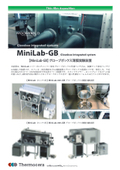
MiniLab-026/090 Glove Box Thin Film Experiment Device


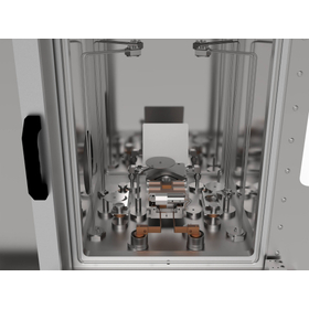
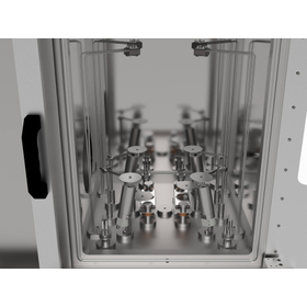
Compact and space-saving! Ideal for organic thin film development, all processes such as deposition, sputtering, and annealing can be seamlessly performed within the glove box.
In the film formation process of 2D materials such as OLED (Organic EL), OPV (Organic Photovoltaic), OTFT (Organic Thin Film Transistor), graphene, and TMD (Transition Metal Dichalcogenides), it is necessary to handle samples in an inert gas atmosphere isolated from oxygen and moisture. The MiniLab-026/090-GB achieves a "oxygen and moisture-free" experimental environment for organic film applications by housing the PVD chamber within the GB, creating a compact and space-saving environment. 【Features】 ◉ A series of processes such as PVD film formation, spin coating, and hot plate baking can be performed seamlessly within the GB without exposing them to the outside air. ◉ Space-saving: The chamber does not protrude from the back, so it does not take up space. 【MiniLab Models】 ◉ MiniLab-026 (26ℓ volume): Metal/insulator/organic material deposition, sputtering, plasma etching, annealing ◉ MiniLab-090 (90ℓ volume): Metal/insulator/organic material deposition, EB deposition, sputtering, plasma etching, annealing * Please first contact us with your required specifications, and we will configure the system according to your needs.
basic information
【GB Compatible MiniLab-026/090 Main Specifications】 ◉ Substrate Size: Maximum Φ6" (026), Maximum Φ10" (090) ◉ Chamber: Made of SUS304, UHV compatible (*090 features a sliding door type, with a maintenance door at the back) ◉ 19-inch control rack stored under the workbench ◉ ML Chamber Internal Film Deposition Module: - Resistance heating evaporation source (up to 4 sources) - Organic evaporation source (up to 4 sources) - Φ2" Magnetron cathodes (up to 3 units) - Plasma etching - Substrate heating stage, etc. ◉ High precision film thickness control ◉ Turbo molecular pump + rotary pump (dry scroll pump option) ◉ Other abundant options *For other detailed specifications, please contact us.
Price range
Delivery Time
Model number/Brand name
MiniLab-026/090-GB
Applications/Examples of results
OLED (Organic Electroluminescent) OPV (Organic Photovoltaic) OTFT (Organic Thin-Film Transistor) Graphene 2D Materials (Two-dimensional layered inorganic nanomaterials such as transition metal dichalcogenides) Others
Detailed information
-

TE1 (1-pole) to TE4 (4-pole) resistance heating filament *The photo shows a 3-pole type. It is a base chamber equipped with multiple spare ports, allowing for easy rearrangement and expansion.
-

Basket type thermal source for MiniLab-LT26A resistance heating evaporation device, basket type x4 pole type.
-

Organic material evaporation source cell LTES-1cc or 5cc Organic source cell for MiniLab series Easy to attach and detach the crucible during material replenishment Alumina or quartz crucible Temperature control range 80 to 600°C UHV compatible High-precision PID automatic film thickness loop control is possible with dedicated controllers LTEC-1S (1ch), LTEC-4S (4ch) (±0.1Å/sec)
-

LT26A_Glovebox-system-installed-1 LT26A_Glovebox-system-installed-1
-

LT26A_Glovebox-system-installed-2 LT26A_Glovebox-system-installed-2
Related Videos
catalog(35)
Download All Catalogs











News about this product(50)
-

■□【PyroMini】□■ Compact High-Performance Infrared Temperature Sensor
High-performance touch panel converter for easy setup, data logging, and data storage on microSD card. The PM2.2 model can also measure glossy metal surfaces. 【Overview】 With a highly visible high-brightness touch panel display, parameters such as temperature range, emissivity, and sampling rate can be intuitively operated and set. Long-term data storage and management are possible with a microSD card. (*An option for a converter without a display is also available.) The compact sensor head, measuring φ18mm x 45mm, allows for temperature measurement in tight spaces. It employs sensors and cables with excellent noise resistance, making it suitable for integration into moving equipment such as robotic arms. The PM2.2 model uses a short wavelength of 2.2um, supporting high temperatures (Max 2000℃) and measurements of glossy metal material surfaces. 【Features】 ◎ Wide range: -20 to 1000℃ (PM), 100 to 2000℃ (PM2.2) ◎ Excellent basic performance: Accuracy ±1%, reproducibility ±0.5%, 240msec fast response ◎ Measurement wavelength range: 8 to 14μm (PM), 2.0 to 2.2μm (PM2.2) ◎ Compact Φ18mm x 45mm
-
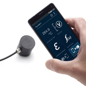
★★【PyroNFC】Smartphone Configurable Infrared Radiation Temperature Sensor★★
Temperature range, emissivity, alarm, and other parameters can be set using a smartphone or tablet without the need for a display instrument or power supply for the instrument. ● Settings can be made using a smartphone or tablet. ● A dedicated app can be downloaded for free from Google Play (Android 4.1 to 5.1). ● Using Android's NFC communication, simply touch the sensor part to read and write data. ● Ultra-compact sensor (Φ31mm x t29mm) allows temperature measurement in tight spaces. ● Fast response time of 125 msec, high accuracy of ±1.5%. ● Voltage output (0-5V or 0-10V), or K thermocouple output. 【Other Specifications】 ◉ Field of view: 15:1 ◉ Temperature range: 0℃ to 1000℃ ◉ Measurement wavelength range: 8 to 14μm ◉ Emissivity: 0.2 to 1.0 ◉ Power supply: 24VDC (minimum 6V/10V to maximum 28VDC) ◉ Cable: 1m included (extension up to 30m possible) 【Options】 ◉ Body mounting bracket ◉ Extension cable ◉ Air purge kit
-

■□【PyroCouple】□■ Small Non-Contact Infrared Temperature Sensor
Compact measurement, robust body, high accuracy ±1%, 240msec fast response. It can be applied for industrial machine control, temperature monitoring in production sites, and various other purposes. 【Features】 ◎ Integrated amplifier and sensor ◎ 4-20mA output (standard), 0-50mV, thermocouple K, J, T output (optional) ◎ Accuracy: ±1% or ±1℃ (whichever is larger) ◎ Repeatability: ±0.5% or ±0.5℃ (whichever is larger) ◎ Response speed: 240msec ◎ Protection rating: IP65 【Other Specifications】 ◉ Field of view: 2:1 or 15:1 ◉ Temperature range: ・LT (-20℃ to 100℃) ・MT (0 to 250℃) ・HT (0 to 500℃) ◉ Measurement wavelength range: 8 to 14μm ◉ Emissivity: 0.95 (fixed) ◉ Power supply: 24VDC ◉ Body dimensions: Φ18mm (diameter) x 103mm (length) ◉ Weight: approximately 95g ◉ Cable 1m (standard included): maximum extension 3m (optional)
-

■□【PyroUSB】□■ USB-connected high-precision infrared temperature sensor
【Overview】 Connect to a Windows PC using the standard accessory "CalexConfig" and the included USB cable (1.8m), allowing you to set measurement parameters for the sensor, analyze measurement results, and output them in CSV format. 1) 4-20mA output 2) USB output (operates on USB bus power) 3) Simultaneous use of 4-20mA/USB output These three methods of use are possible. 【Features】 ◎ Simultaneous use of USB data logging and 4-20mA analog output ◎ Excellent basic performance: accuracy ±1%, reproducibility ±0.5%, 200msec fast response ◉ PUA2: Covers short wavelengths from 2.0 to 2.4μm, capable of measuring metal surfaces ◉ PUA5: Optimal for measuring glass surfaces, wavelength 5μm ◉ PUA8: General-purpose, suitable for a wide range of applications, wavelength 8-14μm 【Other Specifications】 ◉ Field of view: 15:1, 25:1, 30:1, or 75:1 ◉ Emissivity setting range: 0.1 to 1.0 ◉ Power supply: 24VDC ◉ Body dimensions: Φ27.6mm (diameter) x 61mm (length) ◉ Weight: approximately 155g ◉ Analog signal cable 1m (standard included, extendable up to 30m) *USB cable 1.8m (USB cable cannot be extended)
-
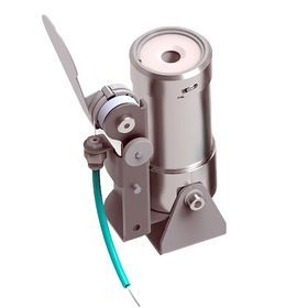
◆OLED◆ Organic vapor deposition - High-temperature metal evaporation source Max 1500℃
The OLED evaporation source is a high-temperature heating heater for vacuum devices with a maximum operating temperature of 1500°C. It can evaporate materials with high evaporation temperatures, making it suitable for a wide range of applications as a vacuum high-temperature heater and evaporation cell, from low-temperature organic deposition (up to 800°C) cells to high-temperature resistance heating deposition (up to 1500°C) MBE cells. Shutter actuators and water-cooled jackets are also available. High-temperature heaters above 800°C are designed with internal shielding, considering insulation and thermal shielding. 【Main Specifications】 ■ Maximum control temperature: 800°C or 1500°C ■ Operating environment: in vacuum or inert gas (*O2 up to 800°C) ■ Heater: tungsten filament ■ Crucible volume: 1cc (maximum fill volume 1.5cc) ■ Crucible material: alumina ■ Case material: SUS304 or molybdenum ■ Thermocouple: K or C 【Options】 ⚫ Crucible material: PBN, graphite, quartz ⚫ Heater: NiCr wire, Kanthal wire (*for O2) ⚫ Crucible volume: 10cc (maximum fill volume 15cc) ⚫ Shutter: pneumatic or motor-driven ⚫ Water-cooled jacket ⚫ Controller (for heater and shutter control)
Recommended products




Distributors

【Endless possibility_thermal engineering...】 Our company sells vacuum thin film devices for semiconductor and electronic device fundamental research, ultra-high temperature heaters for CVD substrate heating, experimental furnaces, temperature measurement equipment, and more. To meet the endless demand for "heat," which is indispensable in any era, and to respond to various requests in the field of fundamental technology development, we aim to introduce the latest equipment and contribute to research and development in Japan.