
Vacuum deposition device 'MiniLab-090' (for glove box)


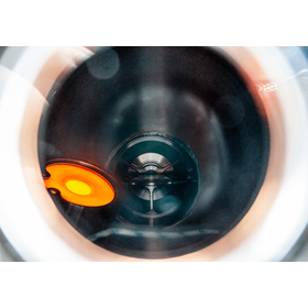


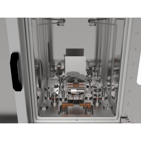
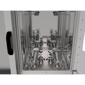
Storage-compatible glove box PVD flexible thin film experimental device, featuring a tall chamber with a height of 570mm, contributes to improved uniformity during deposition.
MiniLab-080 glove box model with an 80ℓ large capacity chamber designed to be stored within a glove box bench. It features a slide-open and close chamber that maximizes the use of the workbench, and a rear-opening door designed with maintenance in mind. Samples processed can be consistently handled within a controlled environment inside the glove box without exposure to the atmosphere or moisture. For specifications of the GB gas purification unit, please refer to the GB model. ◉ Resistance heating evaporation source x up to 4 ◉ Organic evaporation source x up to 4 ◉ Magnetron sputtering cathode x 4 ◉ Electron beam evaporation ◉ Dry etching ◉ Annealing
basic information
【Main Specifications】 - Maximum substrate size: Φ10 inch - SUS304 80ℓ volume 400x400x570mm front-loading chamber - Pump: Turbo molecular pump, rotary pump (dry pump also available) - Vacuum exhaust: Automatic control of vacuum/vent - Resistance heating deposition: Up to 4 sources (Model TE1 to TE4 deposition sources) - Organic deposition: Up to 4 sources (Model LTEC-1cc/5cc) - EB electron beam deposition source: 7cc crucible x 6 (or 4cc crucible x 8) - Φ2 to 4 inch magnetron sputtering cathode x up to 4 - Process control: Manual/automatic continuous multilayer film and simultaneous film formation, APC automatic control - Film thickness monitor: Quartz crystal sensor head x 4 - Film thickness control: Inficon SQM-160 (or SQC-310) 2ch/4ch thin film controller - Utilities: Power supply 200V three-phase 15A, water cooling 3ℓ/min, N2 vent 0.1Mkpa - Other options: Substrate rotation/lifting, plasma etching, dry pump
Price information
This device is a customized product and will vary depending on the configuration, so please inquire for details.
Delivery Time
Model number/Brand name
MiniLab-080
Applications/Examples of results
Various basic experimental applications in university and corporate research laboratories - Optical thin films - Electrode films, semiconductor films, wiring films, insulating films Others
Related Videos
catalog(35)
Download All Catalogs












News about this product(7)
-

【MiniLab】 Evaporation/Sputtering Dual Chamber System
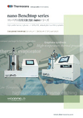
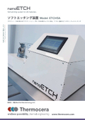
Two thin film experimental devices are connected by a load lock mechanism. Different film deposition devices (sputtering - evaporation, etc.) are seamlessly connected via the load lock. With Moorfield's unique load lock system, connections to the process chamber on the left, right, and rear are also possible (see photo below). 1. MiniLab-E080A (Evaporation Device) - EB evaporation: 7cc crucible x 6 - Resistance heating evaporation x 2 - Organic evaporation limit x 2 2. MiniLab-S060A (Sputtering Device) - Φ2" Magnetron cathode x 4 for simultaneous sputtering - Compatible with both DC and RF power supplies 3. Load Lock Chamber - Plasma etching stage In the load lock chamber, plasma cleaning of the substrate surface is performed using the "RF/DC substrate bias stage," and the company's unique "soft etching" technology allows for a <30W low-power, damage-free plasma etching stage. This enables delicate etching processes that are prone to damage, such as 2D (removal of resists like PMMA), graphene delamination, and etching of Teflon substrates. (*This can also be installed in the main chamber stage.)
-

MiniLab-WCF Ultra High Temperature Wafer Annealing Furnace Max 2000℃_Dedicated for High-Temperature Wafer Sintering (6inch to 8inch)
Max 2000℃ Φ6〜8 inch wafer dedicated high-temperature annealing device, capable of small-scale production multi-atmosphere wafer annealing device. ◾️ Max 2000℃ ◾️ Effective heating range: Φ6〜Φ8 inch single wafer type or batch type (multi-stage 5 wafer cassette) ◾️ Heater control: 1 zone or 2 zones (cascade control) ◾️ Heater materials: ・C/C composite: Φ6〜Φ8 inch ・PG coating high-purity graphite: Φ6〜Φ8 inch ◾️ Operating atmosphere: ・Vacuum (1x10⁻²Pa), inert gas (Ar, N2) ◾️ PLC semi-automatic operation ・Automatic sequence control for vacuum/purge cycle and venting ・Fully automatic operation (optional) ・Touch panel operation, allowing centralized management without dispersed operations. ◾️ Process pressure control ・APC control (MFC flow or automatic opening adjustment valve PID loop control) ・Maximum 3 systems of MFC flow automatic control, or manual adjustment of float meter/needle valve ◾️ PLOT screen graph display, CSV data output
-

4-Yen Multi-Sputtering Device 【MiniLab-S060】
4 cathodes with Φ2 inch configuration Simultaneous film deposition: 3-component simultaneous deposition (RF 500W or DC 850W) + HiPIMS (PulseDC 5KW) x 1 Power distribution and configuration settings for 4 cathodes can be freely changed via the HMI screen using the plasma relay switch 3 MFC systems (Ar, O2, N2) for reactive sputtering RIE etching stage RF 300W (main chamber) + <30W soft etching (LL chamber) Substrate heating: Max 500℃, 800℃, or 1000℃ (C/C or SiC coating) Substrate rotation and vertical movement (automatically controlled by stepping motor) APC automatic control: Upstream (MFC flow adjustment) or downstream (automatic valve opening adjustment on the exhaust side) Dimensions: 1,120(W) x 800(D) ● Mixed specifications for resistance heating deposition, organic material deposition, EB deposition, PECVD, etc. are also possible.
-
![Multisource Simultaneous Sputtering Device [MiniLab-S125]](https://image.mono.ipros.com/public/news/image/1/053/100513/IPROS09263764224142550225.jpeg?w=280&h=280)
Multi-Target Sputtering Device [MiniLab-125] Compatible with Φ8" SiC Coating Equipped with 1000℃ Heater Stage! Compact Size!
Multifunctional Multi-Sputtering Device (Compatible with Φ8inch Substrates) - Simultaneous deposition of three components + one component Pulse DC sputtering - Flexible arrangement of RF500W and DC850W power supplies to three cathodes (Source 1, 2, 3) - Equipped with a 5KW Pulse DC power supply → used with dedicated cathode (4) - Substrate heating stage Max 800℃ (SiC coated heater can achieve Max 1000℃) - MFC x 3 systems (Ar, O2, N2) for reactive sputtering - Main chamber RIE etching stage RF300W - LL chamber <30W low power controlled soft etching - Unique "Soft-Etching" technology reduces substrate damage through substrate bias - Touch panel or Windows PC operation: All operations can be performed on the touch panel/PC without dispersing control. - Equipment installation dimensions: 1,960(W) x 1,100(D) x 1,700(H) mm - Multi-chamber type can also be manufactured. ● Mixed specifications for resistance heating deposition, organic material deposition, EB deposition, PECVD, etc. are also possible.
-

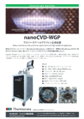
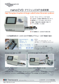
☆★☆★【nanoCVD-WGP】Wafer-scale graphene/carbon nanotube synthesis device ☆★☆★
Plasma CVD equipment compatible with wafer sizes Φ3 inch and Φ4 inch. Rapid synthesis of clean, high-quality graphene while suppressing impurities. Usable with both thermal CVD and low to high temperature plasma CVD methods. The configuration can be customized according to requirements, including mass flow gas supply systems and substrate heating heaters. 【Example of equipment configuration】 - Substrate: Cu, Ni, etc. (film, foil) - Raw materials: CH4, C2H4, solids (PMMA), etc. - Process gases: H2, Ar, N2, etc. - Substrate size: Φ4 inch - 150W, 13.56MHz RF power supply - Substrate heating from 500℃ to Max 1100℃ - High precision process gas pressure APC control - Mass flow controller with a maximum of 4 channels
Recommended products




Distributors

【Endless possibility_thermal engineering...】 Our company sells vacuum thin film devices for semiconductor and electronic device fundamental research, ultra-high temperature heaters for CVD substrate heating, experimental furnaces, temperature measurement equipment, and more. To meet the endless demand for "heat," which is indispensable in any era, and to respond to various requests in the field of fundamental technology development, we aim to introduce the latest equipment and contribute to research and development in Japan.