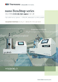
MiniLab Series Flexible Thin Film Experiment Device


Due to its modular embedded design, it is possible to flexibly assemble dedicated equipment according to the required film formation method. A compact thin-film experimental device that can accommodate various research applications.
**Flexible System** The MiniLab thin film experimental device series allows for easy construction of a compact device configuration without waste, even as a customized product, by incorporating suitable components (such as deposition sources and stages) and control modules according to the required deposition methods and materials from a wide range of options. By configuring the device with a modular control unit in a Plug&Play manner, the application range expands, enabling various thin film process experiments. The MiniLab series is a high cost-performance system that caters to a wide range of applications from research and development to small-scale production. **Small Footprint & Space Saving** - Single Rack Type (MiniLab-026): 590(W) x 590(D)mm - Dual Rack Type (MiniLab-060): 1200(W) x 590(D)mm - Triple Rack Type (MiniLab-125): 1770(W) x 755(D)mm **Excellent Operability & Intuitive Operation Screen** Windows PC or 7” touch panel. Easy operation that does not require advanced skills, while ensuring maximum safety.
basic information
【MiniLab Flexible Thin Film Experimental Device Configuration Modules】 ◉ Manufacturing Range Resistance Heating Deposition (TE), Organic Film Deposition (LTE), Electron Beam Deposition (EB), RF/DC Sputtering (SP), T-CVD/PE-CVD, Plasma Etching (RIE) ◉ Chambers ・026 (26 Liters) - TE/LTE/SP/CVD/Etch/*Globe Box option: Max Φ6 inch ・060 (60 Liters) - TE/LTE/EB/SP/Etch/: Max Φ8 inch ・080 (80 Liters) - TE/LTE/EB/SP/Etch/: Max Φ10 inch ・090 (90 Liters) *Globe Box option - TE/LTE/EB/SP/Etch/: Max Φ10 inch ・125 (125 Liters) - TE/LTE/EB/SP/Etch/CVD: Max Φ12 inch * For other specifications, please refer to our website.
Price information
Please feel free to contact us.
Delivery Time
Applications/Examples of results
Main uses: - Development of new materials - Advanced technology development - Small-scale prototype production and so on.
Related Videos
catalog(37)
Download All Catalogs


News about this product(60)
-

High-Temperature Annealing Furnace ◉ Mini-BENCH-prism Semi-Automatic Ultra-High Temperature Experimental Furnace Max 2000℃
◉ Maximum operating temperature Max 2000℃ ◉ PLC semi-auto control A higher model of the tabletop Mini-BENCH with semi-auto control Automatically controls each process of "vacuum/purge cycle," "gas replacement," and "venting" Maximum operating temperature 2000℃ Semi-auto control ultra-high temperature experimental furnace (carbon furnace, tungsten metal furnace) Compact and space-saving experimental furnace ◉ Effective heating range (crucible dimensions) - Flat heater heating range: Φ2 inch to Φ6 inch - Cylindrical heater heating range: Φ30 to Φ80 x Depth Max 100(H) mm ◉ Up to 3 MFC systems for automatic flow control (or manual adjustment) ◉ APC automatic pressure control ◉ Ensures safety during operation Monitors abnormal cooling water, chamber temperature, and overpressure. Made of SUS, robust water-cooled chamber can be safely used even during continuous operation at maximum temperature. ◉ Compact and space-saving Width 603 x Depth 603 x Height 1,160 mm (*Installed inside rotary pump housing) Ultra-high temperature heating experiments for small samples in the laboratory, as well as various sample heating experiments for new material research and development, can be easily conducted with simple operations. The main unit is compact yet can be used for research and development in various fields.
-

◉Mini-BENCH-prism Semi-Automatic Ultra-High Temperature Experimental Furnace Max 2000℃
◉ Maximum operating temperature Max 2000℃ ◉ PLC semi-automatic control A higher model of the tabletop Mini-BENCH with semi-automatic control Automatically controls each process of "vacuum/purge cycle," "gas replacement," and "venting" Maximum operating temperature 2000℃ Semi-automatic control ultra-high temperature experimental furnace (carbon furnace, tungsten metal furnace) Compact and space-saving experimental furnace ◉ Effective heating range (crucible dimensions) - Planar heater heating range: Φ2 inch to Φ6 inch - Cylindrical heater heating range: Φ30 to Φ80 x Depth Max 100(H) mm ◉ Up to 3 MFC systems for automatic flow control (or manual adjustment) ◉ APC automatic pressure control ◉ Ensures safety during operation Monitors abnormal cooling water, chamber temperature, and overpressure. Made of SUS, the robust water-cooled chamber can be safely used even during continuous operation at maximum temperature. ◉ Compact and space-saving Width 603 x Depth 603 x Height 1,160 mm (*Installed inside rotary pump housing) Various sample heating experiments, such as ultra-high temperature heating of small samples and new material research and development, can be easily performed with simple operations. The main unit is compact yet can be used for research and development in various fields.
-

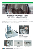
4-Yen Multi-Sputtering Device 【MiniLab-S060】
4 cathodes with Φ2 inch configuration Simultaneous film deposition: 3-component simultaneous deposition (RF 500W or DC 850W) + HiPIMS (PulseDC 5KW) x 1 Power distribution and configuration settings for 4 cathodes can be freely changed via the HMI screen using the plasma relay switch 3 MFC systems (Ar, O2, N2) for reactive sputtering RIE etching stage RF 300W (main chamber) + <30W soft etching (LL chamber) Substrate heating: Max 500℃, 800℃, or 1000℃ (C/C or SiC coating) Substrate rotation and vertical movement (automatically controlled by stepping motor) APC automatic control: Upstream (MFC flow adjustment) or downstream (automatic valve opening adjustment on the exhaust side) Dimensions: 1,120(W) x 800(D) ● Mixed specifications for resistance heating deposition, organic material deposition, EB deposition, PECVD, etc. are also possible.
-

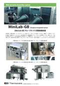
★☆★☆【MiniLab-026】Small Thin Film Experimental Device for R&D Development★☆★☆
This is a flexible thin film experimental device for R&D that eliminates waste by integrating the necessary minimum modules and controllers into a 19" compact rack with a Plug & Play feel, achieving compact size, space-saving design, simple operation, and high cost performance. It supports magnetron sputtering (up to 3 sources) or resistance heating evaporation (metal sources up to 2, organic materials x4), and can also be equipped with a substrate heating stage, allowing for the production of annealing devices and RF etching. There is also a glove box storage type available (specifications to be discussed). We offer a wide range of optional components that can be flexibly customized. ◉ Φ2 inch magnetron cathode (up to 3 sources) ◉ Resistance heating evaporation source filament, crucible, boat type (up to 4 poles with automatic switching via controller) ◉ Organic evaporation cell: 1cc or 5cc ◉ Glove box compatible (optional, specifications to be discussed) ◉ Other options: simultaneous film deposition, HiPIMS, automatic film deposition controller, custom substrate holders, load lock, substrate rotation/heating/cooling, and many more options available. *Please first contact us with your required specifications, and we will configure the system to meet your needs.
-

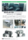
★☆★☆【MiniLab-026】Flexible Thin Film Experimental Device for R&D★☆★☆
This is a flexible thin-film experimental device for R&D that achieves minimal waste, compact size, simple operation, and high cost performance by integrating the necessary minimum modules and controllers into a 19" compact rack with a Plug&Play feel. It supports magnetron sputtering (up to 3 sources) or resistance heating evaporation (metal sources up to 2, organic materials x4), and can be equipped with a substrate heating stage, allowing for the production of annealing devices and RF etching. A glove box storage type is also available (specifications to be discussed). We offer a wide range of optional components that can be flexibly customized. ◉ Φ2 inch magnetron cathode (up to 3 sources) ◉ Resistance heating evaporation source filament, crucible, boat type (up to 4 poles with automatic switching via controller) ◉ Organic evaporation cell: 1cc or 5cc ◉ Can be equipped with a glove box (optional, specifications to be discussed) ◉ Other options: Simultaneous film deposition, HiPIMS, automatic film deposition controller, custom substrate holders, load lock, substrate rotation/heating/cooling, and many other options available. *Please first contact us with your required specifications, and we will configure the system according to your needs.
Recommended products


Distributors

【Endless possibility_thermal engineering...】 Our company sells vacuum thin film devices for semiconductor and electronic device fundamental research, ultra-high temperature heaters for CVD substrate heating, experimental furnaces, temperature measurement equipment, and more. To meet the endless demand for "heat," which is indispensable in any era, and to respond to various requests in the field of fundamental technology development, we aim to introduce the latest equipment and contribute to research and development in Japan.