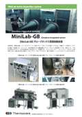
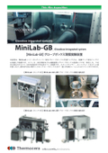
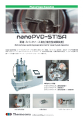
Sputtering device "MiniLab series"


Due to its modular embedded design, it is possible to flexibly assemble dedicated equipment according to the required film deposition method. A compact thin-film experimental device that can accommodate various research applications.
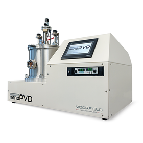
**Flexible System** The MiniLab thin film experimental device series allows for easy construction of a compact system without waste, even as a customized product, by incorporating suitable components (such as deposition sources and stages) and control modules according to the required deposition methods and materials from a wide range of options. By configuring the device with a modular control unit in a Plug&Play manner, the application range expands, enabling various thin film process experiments. The MiniLab series is a high-cost performance system that caters to a wide range of applications from research and development to small-scale production. **Small Footprint & Space-Saving** - Single Rack Type (MiniLab-026): 590(W) x 590(D)mm - Dual Rack Type (MiniLab-060): 1200(W) x 590(D)mm - Triple Rack Type (MiniLab-125): 1770(W) x 755(D)mm **Excellent Operability & Intuitive Operation Screen** Windows PC or 7” touch panel. Easy operation that does not require advanced skills, while ensuring maximum safety.
basic information
【MiniLab Flexible Thin Film Experimental Device Configuration Modules】 ◉ Manufacturing Range Resistance Heating Deposition (TE), Organic Film Deposition (LTE), Electron Beam Deposition (EB), RF/DC Sputtering (SP), T-CVD/PE-CVD, Plasma Etching (RIE) ◉ Chambers ・026 (26 Liters) - TE/LTE/SP/CVD/Etch/*Globe Box option: Max Φ6 inch ・060 (60 Liters) - TE/LTE/EB/SP/Etch/: Max Φ8 inch ・080 (80 Liters) - TE/LTE/EB/SP/Etch/: Max Φ10 inch ・090 (90 Liters) *Globe Box option - TE/LTE/EB/SP/Etch/: Max Φ10 inch ・125 (125 Liters) - TE/LTE/EB/SP/Etch/CVD: Max Φ12 inch * For other specifications, please refer to our website.
Price information
Please feel free to contact us.
Delivery Time
Applications/Examples of results
Main uses: - Development of new materials - Advanced technology development - Small-scale prototype production etc.
Related Videos
catalog(37)
Download All Catalogs


News about this product(8)
-

4-Yen Multi-Sputtering Device 【MiniLab-S060】
4 cathodes with Φ2 inch configuration Simultaneous film deposition: 3-component simultaneous deposition (RF 500W or DC 850W) + HiPIMS (PulseDC 5KW) x 1 Power distribution and configuration settings for 4 cathodes can be freely changed via the HMI screen using the plasma relay switch 3 MFC systems (Ar, O2, N2) for reactive sputtering RIE etching stage RF 300W (main chamber) + <30W soft etching (LL chamber) Substrate heating: Max 500℃, 800℃, or 1000℃ (C/C or SiC coating) Substrate rotation and vertical movement (automatically controlled by stepping motor) APC automatic control: Upstream (MFC flow adjustment) or downstream (automatic valve opening adjustment on the exhaust side) Dimensions: 1,120(W) x 800(D) ● Mixed specifications for resistance heating deposition, organic material deposition, EB deposition, PECVD, etc. are also possible.
-

Multi-functional Sputtering System 【MiniLab-S060】
4 cathodes with Φ2 inch mounted Simultaneous film formation: 3-component simultaneous film formation (RF 500W or DC 850W) + HiPIMS (PulseDC 5KW) x 1 Power distribution and configuration settings for 4 cathodes can be freely changed from the HMI screen using the plasma relay switch 3 MFC systems (Ar, O2, N2) for reactive sputtering RIE etching stage RF 300W (main chamber) + <30W soft etching (LL chamber) Substrate heating: Max 500℃, 800℃, or 1000℃ (C/C or SiC coat) Substrate rotation and vertical movement (automatically controlled by stepping motor) APC automatic control: Upstream (MFC flow adjustment) or downstream (automatic valve opening adjustment on the exhaust side) Dimensions: 1,120(W) x 800(D) ● Mixed specifications for resistance heating deposition, organic material deposition, EB deposition, PECVD, etc. are also possible.
-

【MiniLab】 Evaporation/Sputtering Dual Chamber System
Two thin film experimental devices are connected by a load lock mechanism. Different film deposition devices (sputtering - evaporation, etc.) are seamlessly connected via the load lock. With Moorfield's unique load lock system, connections to the process chamber on the left, right, and rear are also possible (see photo below). 1. MiniLab-E080A (Evaporation Device) - EB evaporation: 7cc crucible x 6 - Resistance heating evaporation x 2 - Organic evaporation limit x 2 2. MiniLab-S060A (Sputtering Device) - Φ2" Magnetron cathode x 4 for simultaneous sputtering - Compatible with both DC and RF power supplies 3. Load Lock Chamber - Plasma etching stage In the load lock chamber, plasma cleaning of the substrate surface is performed using the "RF/DC substrate bias stage," and the company's unique "soft etching" technology allows for a <30W low-power, damage-free plasma etching stage. This enables delicate etching processes that are prone to damage, such as 2D (removal of resists like PMMA), graphene delamination, and etching of Teflon substrates. (*This can also be installed in the main chamber stage.)
-
![Multisource Simultaneous Sputtering Device [MiniLab-S125]](https://image.mono.ipros.com/public/news/image/1/053/100513/IPROS09263764224142550225.jpeg?w=280&h=280)
Multi-Target Sputtering Device [MiniLab-125] Compatible with Φ8" SiC Coating Equipped with 1000℃ Heater Stage! Compact Size!
Multifunctional Multi-Sputtering Device (Compatible with Φ8inch Substrates) - Simultaneous deposition of three components + one component Pulse DC sputtering - Flexible arrangement of RF500W and DC850W power supplies to three cathodes (Source 1, 2, 3) - Equipped with a 5KW Pulse DC power supply → used with dedicated cathode (4) - Substrate heating stage Max 800℃ (SiC coated heater can achieve Max 1000℃) - MFC x 3 systems (Ar, O2, N2) for reactive sputtering - Main chamber RIE etching stage RF300W - LL chamber <30W low power controlled soft etching - Unique "Soft-Etching" technology reduces substrate damage through substrate bias - Touch panel or Windows PC operation: All operations can be performed on the touch panel/PC without dispersing control. - Equipment installation dimensions: 1,960(W) x 1,100(D) x 1,700(H) mm - Multi-chamber type can also be manufactured. ● Mixed specifications for resistance heating deposition, organic material deposition, EB deposition, PECVD, etc. are also possible.
-
![Multisource Simultaneous Sputtering Device [MiniLab-S125]](https://image.mono.ipros.com/public/news/image/1/761/107145/IPROS11123125483883126633.jpeg?w=280&h=280)
Sputtering/Dual Chamber System【MiniLab-E080A/S060A】
Two thin-film experimental devices are connected via a load lock mechanism. Different film deposition devices (sputtering - evaporation, etc.) are seamlessly connected through the load lock. With Moorfield's unique load lock system, connections to the left, right, and rear process chambers are also possible (see photo below). 1. MiniLab-E080A (Evaporation Device) - EB Evaporation: 7cc crucible x 6 - Resistance Heating Evaporation x 2 - Organic Evaporation Limit x 2 2. MiniLab-S060A (Sputtering Device) - Φ2" Magnetron Cathode x 4 sources for simultaneous sputtering - Compatible with both DC and RF power supplies 3. Load Lock Chamber - Plasma Etching Stage In the load lock chamber, plasma cleaning of the substrate surface is performed using the "RF/DC substrate bias stage," and the company's unique 'soft etching' technology allows for a <30W low-power, damage-free plasma etching stage. This enables delicate etching processes that are prone to damage, such as 2D (removal of resists like PMMA), graphene delamination, and etching of Teflon substrates. (*This can also be installed in the main chamber stage.)
Recommended products


Distributors

【Endless possibility_thermal engineering...】 Our company sells vacuum thin film devices for semiconductor and electronic device fundamental research, ultra-high temperature heaters for CVD substrate heating, experimental furnaces, temperature measurement equipment, and more. To meet the endless demand for "heat," which is indispensable in any era, and to respond to various requests in the field of fundamental technology development, we aim to introduce the latest equipment and contribute to research and development in Japan.