
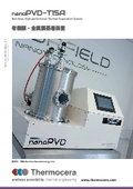
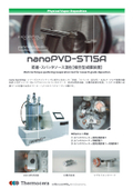
Vacuum Deposition Device "nanoPVD-T15A"


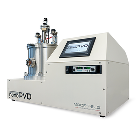
We have incorporated all the latest vacuum deposition technology into a compact benchtop-sized device that can effectively utilize limited lab space.
High-performance organic source LTE (up to 4 sources) with excellent temperature responsiveness/stability for organic materials such as OLED, OPV, and OTFT, and a metal deposition source TE (up to 2 sources) that allows for easy exchange and maintenance. It can operate in manual mode, as well as in automatic modes for continuous multilayer film deposition and simultaneous film deposition. Despite its compact size, it achieves performance similar to that of standalone large machines without sacrificing basic performance, film quality, uniformity, or operability. Additionally, it features fully automated control via a simple touch panel with PLC. The user-friendly HMI allows anyone to operate it intuitively without requiring complicated operating procedures. It comes with remote software "IntelliLink," which connects to a Windows PC via USB cable, enabling monitoring of the device's operating status, log saving, online/offline recipe creation and saving, and fault analysis. This compact vacuum deposition system is designed to maximize the effective use of limited development and lab space while also excelling in maintenance.
basic information
◉Dimensions: 804(W) x 530(D) x 600(H)mm ◉Weight: 40kg to 70kg (depending on equipment configuration) ◉Excellent basic performance ・Achievable vacuum level 5x10⁻⁵ Pascal ・Equipped with high-performance turbo molecular pump ・Up to Φ4 inch substrate ◉Evaporation sources ・Metal evaporation source TE x up to 2 units ・Organic evaporation source LTE x up to 4 units (if mixed with resistive heating TE, up to 2 units) ◉7" touch panel ◉Continuous film deposition ・Automatic control of deposition program ・30 types of recipes registered ・High-precision wide-range vacuum gauge ◉Rich options ・Substrate rotation ・Up and down movement with 300mm stroke ・Substrate shutter ・Dry pump (RP standard) ・Connect to Windows PC via USB for log storage and management
Price information
Please contact us.
Delivery Time
Model number/Brand name
nanoPVD-T15A
Applications/Examples of results
- Development of organic thin films such as OLED, OPV, and OTFT - Industrial applications of optical thin films and decorative films - Development of thin films for electronic substrates and semiconductor substrates - Development of coating materials and thin film materials
Related Videos
catalog(34)
Download All Catalogs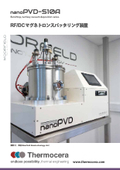








News about this product(5)
-

VOXIA compact X-ray CT imaging device
Compact design with a space-saving layout that can be installed anywhere. Despite its compact body, it generates high-resolution data through advanced calculation software. * X-ray tube voltage: 20-90kV, or 40-maximum 130kV * Focus diameter: 7μm (5μm@4W) * Detector pixel: 89μm, approximately 3.2 million pixels! * Sample size: Φ120mm ◉ Vcap (Control Software): A custom-made imaging stage tailored to the subject and purpose. A series of tasks from shooting to image output can be performed with just a click. High-speed continuous shooting in as fast as 20 seconds, with processing from shooting start to image reconstruction taking about 30 seconds. ◉ VCT (Reconstruction Software): Customizable automatic measurement and analysis software specialized for the specified subject. High-speed reconstruction of shooting data with 992 x 992 pixel images and 600 projections in just 3.8 seconds! ◉ MolcerPlus (3D Display Analysis): Custom software that enables measurement conditions that were difficult with conventional software. Software for displaying, processing, and measuring the imaged object. ● High safety, ● Compatible with a wide variety of samples, ● Intuitive HMI, easy operation.
-

4-Yen Multi-Sputtering Device 【MiniLab-S060】
4 cathodes with Φ2 inch configuration Simultaneous film deposition: 3-component simultaneous deposition (RF 500W or DC 850W) + HiPIMS (PulseDC 5KW) x 1 Power distribution and configuration settings for 4 cathodes can be freely changed via the HMI screen using the plasma relay switch 3 MFC systems (Ar, O2, N2) for reactive sputtering RIE etching stage RF 300W (main chamber) + <30W soft etching (LL chamber) Substrate heating: Max 500℃, 800℃, or 1000℃ (C/C or SiC coating) Substrate rotation and vertical movement (automatically controlled by stepping motor) APC automatic control: Upstream (MFC flow adjustment) or downstream (automatic valve opening adjustment on the exhaust side) Dimensions: 1,120(W) x 800(D) ● Mixed specifications for resistance heating deposition, organic material deposition, EB deposition, PECVD, etc. are also possible.
-
![Multisource Simultaneous Sputtering Device [MiniLab-S125]](https://image.mono.ipros.com/public/news/image/1/053/100513/IPROS09263764224142550225.jpeg?w=280&h=280)
Multi-Target Sputtering Device [MiniLab-125] Compatible with Φ8" SiC Coating Equipped with 1000℃ Heater Stage! Compact Size!
Multifunctional Multi-Sputtering Device (Compatible with Φ8inch Substrates) - Simultaneous deposition of three components + one component Pulse DC sputtering - Flexible arrangement of RF500W and DC850W power supplies to three cathodes (Source 1, 2, 3) - Equipped with a 5KW Pulse DC power supply → used with dedicated cathode (4) - Substrate heating stage Max 800℃ (SiC coated heater can achieve Max 1000℃) - MFC x 3 systems (Ar, O2, N2) for reactive sputtering - Main chamber RIE etching stage RF300W - LL chamber <30W low power controlled soft etching - Unique "Soft-Etching" technology reduces substrate damage through substrate bias - Touch panel or Windows PC operation: All operations can be performed on the touch panel/PC without dispersing control. - Equipment installation dimensions: 1,960(W) x 1,100(D) x 1,700(H) mm - Multi-chamber type can also be manufactured. ● Mixed specifications for resistance heating deposition, organic material deposition, EB deposition, PECVD, etc. are also possible.
-

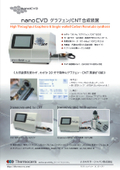
☆★☆★【nanoCVD-WGP】Wafer-scale graphene/carbon nanotube synthesis device ☆★☆★
Plasma CVD equipment compatible with wafer sizes Φ3 inch and Φ4 inch. Rapid synthesis of clean, high-quality graphene while suppressing impurities. Usable with both thermal CVD and low to high temperature plasma CVD methods. The configuration can be customized according to requirements, including mass flow gas supply systems and substrate heating heaters. 【Example of equipment configuration】 - Substrate: Cu, Ni, etc. (film, foil) - Raw materials: CH4, C2H4, solids (PMMA), etc. - Process gases: H2, Ar, N2, etc. - Substrate size: Φ4 inch - 150W, 13.56MHz RF power supply - Substrate heating from 500℃ to Max 1100℃ - High precision process gas pressure APC control - Mass flow controller with a maximum of 4 channels
-
Vacuum deposition device □■□【MiniLab-LT080A】□■□ Capable of various deposition applications such as resistance heating, organic deposition, and electron beam deposition.
The ML-080, with a volume of 80 liters and dimensions of 400(W)x400(D)x570(H)mm, is composed of a D-type box chamber. It has the same configuration as the 070 model but features a taller chamber, resulting in a longer TS distance adjustment range and improved film uniformity during deposition on large-diameter substrates, making it an optimal model for vacuum deposition. It is a higher-end model than the ML-070, which can also accommodate a load lock mechanism. Like the 070, it is compact yet supports a wide range of applications including resistance heating deposition (for metals, insulators, and organic materials), electron beam deposition, RF/DC/PulseDC compatible magnetron sputtering, RIE plasma etching, and annealing. - Maximum substrate size: Φ11 inch - Resistance heating deposition source x up to 4 units - Organic deposition source x up to 4 units - Magnetron sputtering cathode x 4 units - Electron beam deposition - Substrate heating stage (standard 500℃, Max 1000℃) - *Plasma etching / <30W soft etching *Plasma etching can be installed in both the main chamber and the load lock chamber.
Recommended products




Distributors

【Endless possibility_thermal engineering...】 Our company sells vacuum thin film devices for semiconductor and electronic device fundamental research, ultra-high temperature heaters for CVD substrate heating, experimental furnaces, temperature measurement equipment, and more. To meet the endless demand for "heat," which is indispensable in any era, and to respond to various requests in the field of fundamental technology development, we aim to introduce the latest equipment and contribute to research and development in Japan.